Semiconductor laser device driving circuit

A driving circuit and laser technology, which is applied to semiconductor lasers, lasers, laser components, etc., can solve the problems of not being suitable for laser fuzes, etc., and achieve the effect of adjustable stability and output voltage

Active Publication Date: 2013-07-31
INST OF SEMICONDUCTORS - CHINESE ACAD OF SCI
View PDF2 Cites 24 Cited by
  • Summary
  • Abstract
  • Description
  • Claims
  • Application Information

AI Technical Summary

Problems solved by technology

For the semiconductor laser drive circuit, although the pulse width can reach 5ns, it needs an external 50V high voltage power supply
In addition, there are other examples of driving circuits, the output current (power) is very large but the pulse width is on the order of several microseconds, which is

Method used


Image

  • Semiconductor laser device driving circuit
  • Semiconductor laser device driving circuit
  • Semiconductor laser device driving circuit

Examples


Embodiment Construction

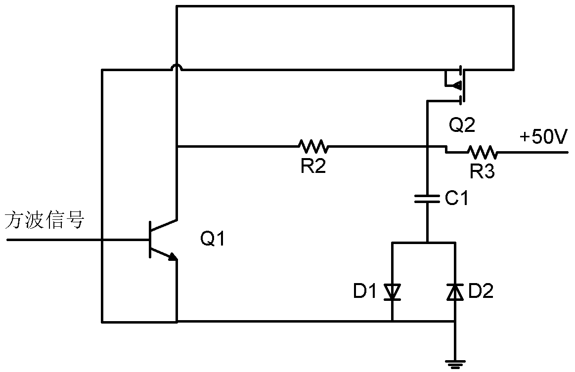
[0024] In order to make the object, technical solution and advantages of the present invention clearer, the present invention will be described in further detail below in conjunction with specific embodiments and with reference to the accompanying drawings. It should be noted that, in the drawings or descriptions of the specification, similar or identical parts all use the same figure numbers. Implementations not shown or described in the accompanying drawings are forms known to those of ordinary skill in the art. Additionally, while illustrations of parameters including particular values ​​may be provided herein, it should be understood that the parameters need not be exactly equal to the corresponding values, but rather may approximate the corresponding values ​​within acceptable error margins or design constraints.

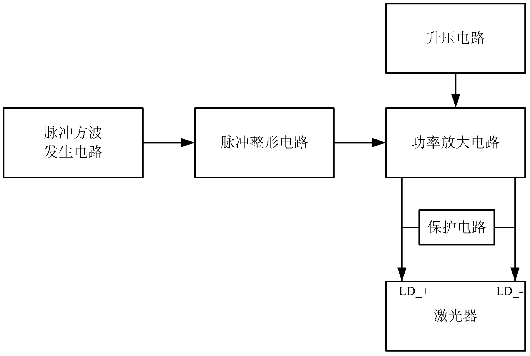
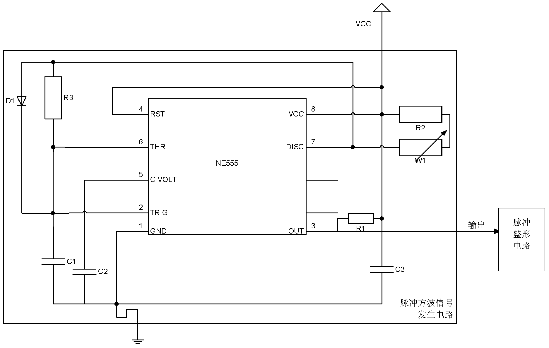
[0025] In an exemplary embodiment of the present invention, a semiconductor laser drive circuit is provided, please refer to figure 2 , The semiconductor las...


PUM

PropertyMeasurementUnit
Fourth capacitoraaaaaaaaaa
Pulse widthaaaaaaaaaa

Abstract

The invention provides a semiconductor laser device driving circuit which comprises a pulse shaping circuit used for shaping a wave form of an input narrow pulse signal and further compressing the pulse width of the narrow pulse signal, and a power amplification circuit connected with the pulse shaping circuit and used for performing power amplification on the narrow pulse signal output by the pulse shaping circuit through using high voltage, and for outputting a high level of the narrow pulse signal to an anode of a laser device and a low level to a cathode of the laser device after the power amplification. According to the semiconductor laser device driving circuit, the pulse width of the narrow pulse signal is further compressed by the pulse shaping circuit, and power of the narrow pulse signal is increased by the power amplification circuit, so that the semiconductor laser device driving circuit can meet requirements of high power and a narrow pulse.

Description

technical field [0001] The invention relates to the technical field of semiconductor lasers, in particular to a semiconductor laser drive circuit. Background technique [0002] With the rapid expansion of the application field of semiconductor lasers, He-Ne lasers are gradually replacing He-Ne lasers in many aspects, and have been widely used in optical fiber communications, integrated optics, laser printing, laser beam scanning, optical disk storage technology, laser ranging, laser radar, pumps, etc. Pump solid-state lasers, pulse Doppler imaging, 3D image systems, fiber optic temperature sensors, etc. In many fields, especially in the field of laser detection and target recognition, the performance of target recognition, ranging accuracy, anti-interference and low power consumption all depend on the quality of laser pulses emitted by semiconductor lasers, and semiconductor lasers emit The optical pulse is directly modulated by the electrical pulse generated by the semicon...

Claims


Application Information

Patent Timeline
IPC IPC(8): H01S5/042
Inventor 彭红玲渠红伟张冶金郑婉华
Owner INST OF SEMICONDUCTORS - CHINESE ACAD OF SCI
Why Eureka
Try Eureka