Memory and storage array thereof, access control method, and access control circuit
A storage array and access control technology, which is applied in the field of memory and its storage array, access control circuit, can solve problems such as occupancy, unfavorable chip size reduction, etc., and achieve the goal of improving storage efficiency, reducing spacing distance, and increasing byte unit density Effect
- Summary
- Abstract
- Description
- Claims
- Application Information
AI Technical Summary
Problems solved by technology
Method used
Image

Examples
Embodiment 1
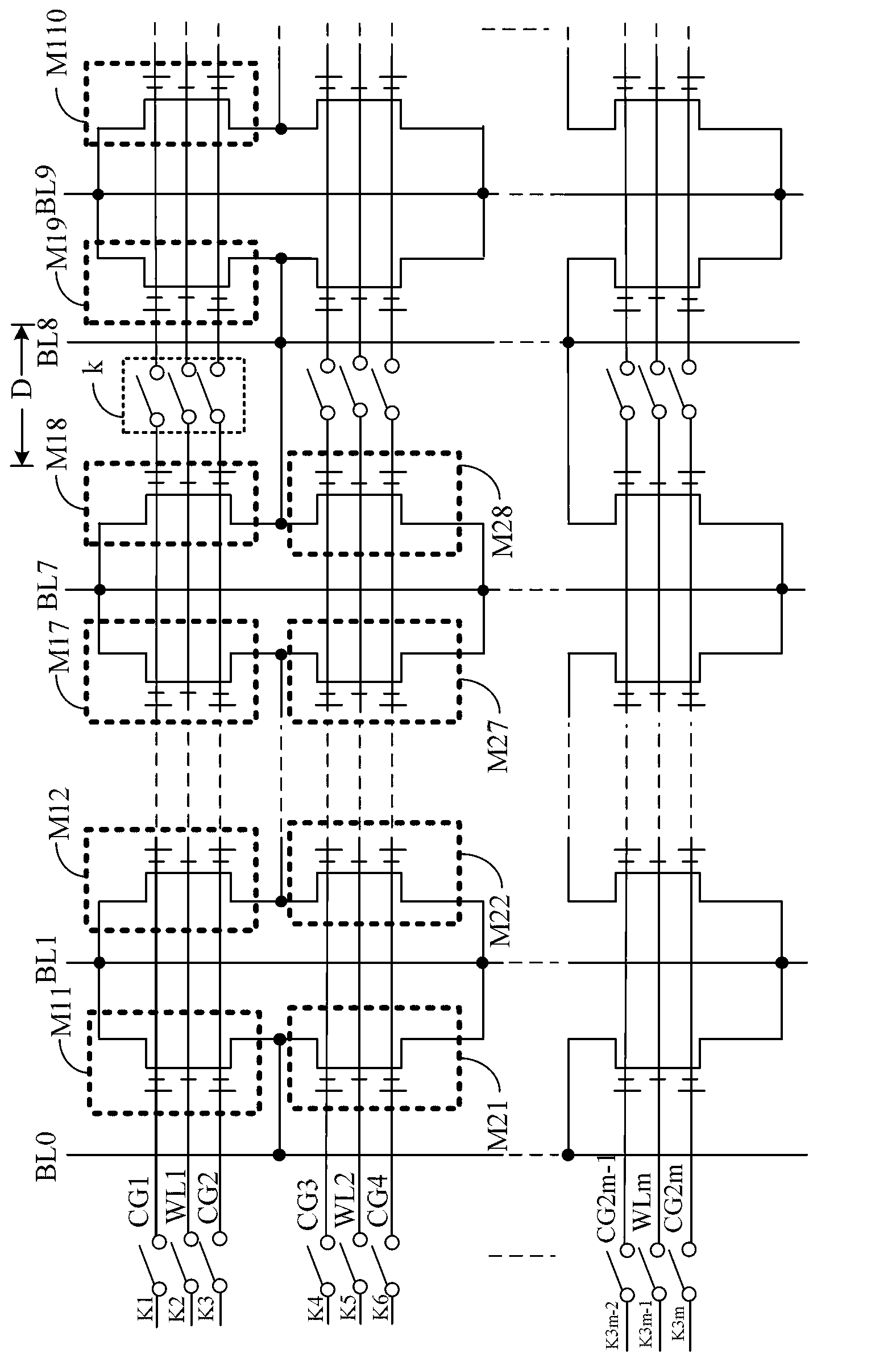
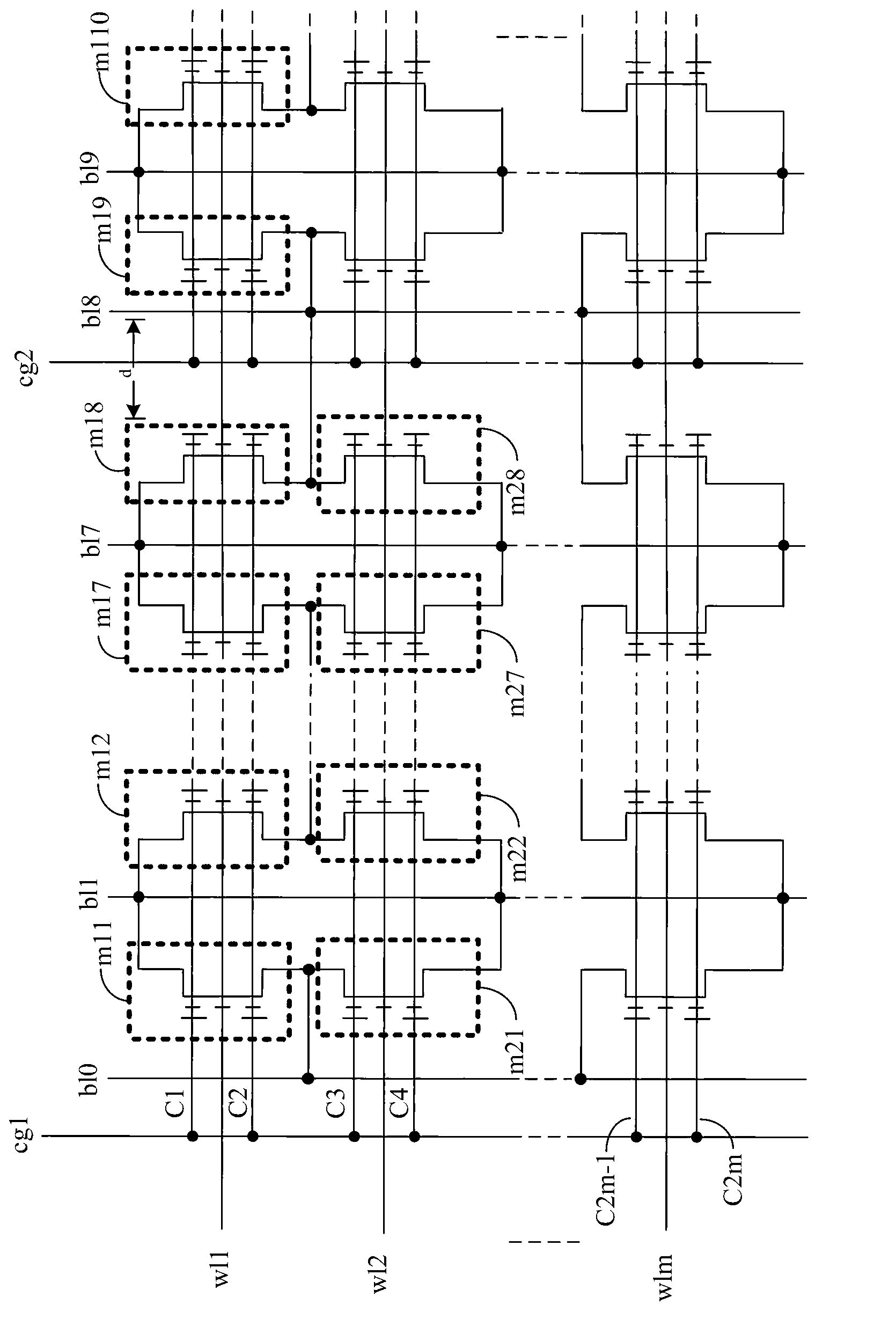
[0052] This embodiment provides a storage array, such as image 3 shown, including:
[0053] A plurality of byte units, where the byte unit includes a plurality of storage units.
[0054] The storage array described in this embodiment includes byte units arranged in a matrix of rows and columns. Here, rows and columns are relative concepts and can be interchanged. like image 3 Among them, let the byte unit composed of storage units m11, m12, ..., m17, m18 be the target byte unit, and the word adjacent to the target byte unit on the same row is composed of storage units m19, m110, ... Section unit, adjacent on the same column as the target byte unit is a byte unit composed of storage units m21, m22, ..., m27, m28, and the present embodiment assumes that the target byte unit is adjacent on the same row The byte unit is a row byte unit, and the byte unit adjacent to the target byte unit on the same column is a column byte unit.
[0055] A plurality of storage cells included ...
Embodiment 2
[0064] Corresponding to the storage array in Embodiment 1, this embodiment provides an access control method for a storage array, including performing the following steps: Figure 5 The steps shown to erase the data in each memory location in the target byte location:
[0065] In step S101, a first word line voltage is applied to word lines connected to memory cells in a target byte unit, and other word lines are set to zero.
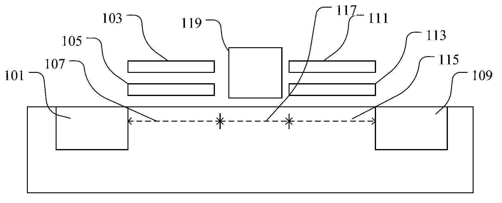
[0066] The value range of the shown first word line voltage may be 6V-9V, combined with figure 1 , the first word line voltage loaded on the first word line charges the middle electrode of each memory cell in the target byte unit to a high driving voltage, so that the middle electrode 119 and the floating gate (the first floating gate 105 or the second floating gate 113 ), a high electric field is generated, and the high electric field can move electrons out of the first floating gate 105 corresponding to the first storage bit or the second floating ga...
Embodiment 3
[0084] A kind of access control circuit corresponding to the storage array of embodiment 2, such as Figure 4 shown. Figure 4 It is a structural schematic diagram of a memory array including several memory blocks and its access control circuit, including memory blocks 11, 21, . . . , 1n, 2n, . . . arranged in a matrix. The structures of each storage block and its access control circuit are similar (the following examples all take the storage block 11 as an example).
[0085] The access control circuit of the storage array in this embodiment includes:
[0086] The word line control unit 1 is used to load the first word line voltage to the word line connected to each memory cell of the target byte unit when performing data erasing on each memory cell in the target byte unit, and to other word lines Zero. The word line control unit 1 includes a plurality of word line control switches respectively connected to corresponding word lines, see Figure 4 , the word line control un...
PUM
 Abstract
Description
Claims
Application Information
 - R&D
- Intellectual Property
- Life Sciences
- Materials
- Tech Scout
- Unparalleled Data Quality
- Higher Quality Content
- 60% Fewer Hallucinations
Browse by: Latest US Patents, China's latest patents, Technical Efficacy Thesaurus, Application Domain, Technology Topic, Popular Technical Reports.
© 2025 PatSnap. All rights reserved.Legal|Privacy policy|Modern Slavery Act Transparency Statement|Sitemap|About US| Contact US: help@patsnap.com