Exposure device and exposure method

一种曝光装置、光干涉的技术,应用在照相制版工艺曝光装置、微光刻曝光设备、光学等方向,能够解决影响曝光装置精度使用的便捷、校准过程复杂等问题,达到减小干扰、提高产量、提高效率和产量的效果

Active Publication Date: 2013-08-14
SEMICON MFG INT (SHANGHAI) CORP
View PDF4 Cites 6 Cited by
  • Summary
  • Abstract
  • Description
  • Claims
  • Application Information

AI Technical Summary

Problems solved by technology

[0009] The positions of the two stages of the existing dual-stage exposure device are difficult to accurately match and control, and the calibration process is relatively complicated, which affects the accuracy of the exposure device (such as overlay accuracy) and the convenience of use

Method used


Image

  • Exposure device and exposure method
  • Exposure device and exposure method
  • Exposure device and exposure method

Examples


Embodiment Construction

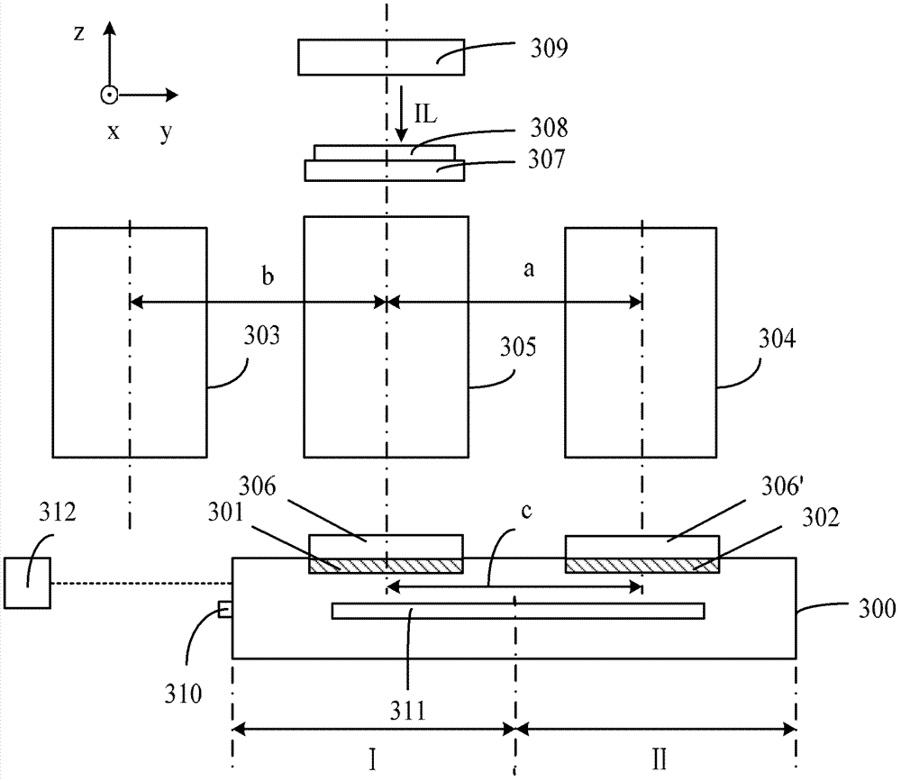
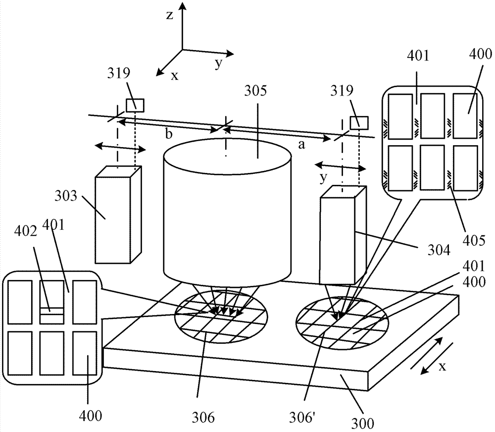
[0055] In the existing dual-stage exposure device, the calibration between the two measurement units of the two stages is complex and difficult, and disturbances are easily generated between the four optical interferometers, making it difficult to accurately position the two stages, affecting the output of the exposure device.

[0056] In order to solve the above problems, the inventor proposes an exposure device, including: a stage, the stage includes a first area and a second area corresponding to the first area, and the stage also includes A first substrate holder and a second substrate holder located in the second region;

[0057] an optical projection unit, located above the stage, for exposing the substrate on the first substrate holder or the second substrate holder;

[0058] The first alignment detection unit and the second alignment detection unit, the first alignment detection unit and the second alignment detection unit are symmetrically distributed on both sides o...


PUM


Abstract

An exposure device and an exposure method are disclosed. The exposure device comprises an objective table which comprises a first area and a second area corresponding to the first area and also comprises a first substrate holder positioned in the first area and a second substrate holder positioned in the second area, an optical projection unit which is positioned above the objective table and is used for exposure of a substrate on the first substrate holder or the second substrate holder, a first alignment check unit and a second alignment check unit which are symmetrically distributed at two sides of the optical projection unit. The first alignment check unit is used for detecting an alignment mark on the substrate on the first substrate holder. The second alignment check unit is used for detecting an alignment mark on the substrate on the second substrate holder. By the adoption of the exposure device provided by the embodiment of the invention, accurate positioning of the objective table is realized, and output of the exposure device is raised.

Description

technical field [0001] The invention relates to the field of semiconductor manufacturing, in particular to an exposure device and an exposure method. Background technique [0002] As a very important process in the semiconductor manufacturing process, photolithography is the process of transferring the pattern on the mask plate to the substrate through exposure, and is considered to be the core step in the manufacture of large-scale integrated circuits. A series of complex and time-consuming photolithography processes in semiconductor manufacturing are mainly completed by corresponding exposure machines. The development of lithography technology or the progress of exposure machine technology mainly revolves around the three major indicators of line width, overlay accuracy and output. [0003] In semiconductor manufacturing, the exposure process mainly includes three major steps: the step of replacing the substrate on the stage; the step of aligning the substrate on the stag...

Claims


Application Information

Patent Timeline
Patent Type & Authority Applications(China)
IPC IPC(8): G03F7/20G03F9/00
CPCG03F7/70725G03F7/70716G03F9/7003
Inventor 伍强郝静安刘畅姚欣李天慧舒强顾一鸣
Owner SEMICON MFG INT (SHANGHAI) CORP
Why Eureka
Try Eureka