OCB type liquid crystal display having transition nucleus area from splay alignment to bend alignment

a liquid crystal display and transition nucleus technology, applied in the field of ocb-type liquid crystal display, can solve the problems of large dependence on viewing angle, large light leakage caused by wavelength dispersion, and low response speed of liquid crystal display of tn system, etc., to achieve easy production and stably maintain the bend alignment condition, maintain the bend alignment, and maintain the bend alignment

Inactive Publication Date: 2005-02-22
VISTA PEAK VENTURES LLC
View PDF8 Cites 19 Cited by
  • Summary
  • Abstract
  • Description
  • Claims
  • Application Information

AI Technical Summary

Benefits of technology

When the angle between each of the slant surfaces of the transition nucleus areas and the substrate is equal to or larger than 45 degrees and when a liquid crystal material used has a ratio of elastic constants of bend alignment and splay alignment k33 / k11 which is equal to or smaller than 1, it is possible to realize bend alignment of the liquid crystal layer in the transition nucleus areas in a condition no voltage is applied between the substrates. Thereby, liquid crystal molecules in other portions of the liquid crystal layer which are splay aligned in a condition no voltage is applied are induced to become bend aligned by the bend alignment condition in the transition nucleus areas, when a voltage is applied between both substrates. Therefore, it becomes possible to easily produce and stably maintain the bend alignment condition in the liquid crystal layer even when a relatively low voltage is applied between both substrates.
Also, when the angle between each of the slant surfaces of the transition nucleus areas and the substrate is equal to or larger than 60 degrees, theoretically in all liquid crystal materials, it is possible to realize bend alignment of the liquid crystal layer in the transition nucleus areas in a condition no voltage is applied between the substrates. The liquid crystal molecules in the transition nucleus areas are bend aligned, even in a condition no voltage is applied between both substrates. Thereby, liquid crystal molecules in other portions of the liquid crystal layer which are splay aligned in a condition no voltage is applied are induced to become bend aligned by the bend alignment condition in the transition nucleus areas, when a voltage is applied between both substrates. Therefore, it becomes possible to easily produce and stably maintain the bend alignment condition in the liquid crystal layer even when a relatively low voltage is applied between both substrates.
Depending on an angle of the slant surface of each transition nucleus area with respect to the substrate, the liquid crystal molecules disposed between the transition nucleus areas become bend aligned. Therefore, even when the pretilt angle of the substrate surface of each of the transition nucleus areas is zero (0) degree, it is possible to maintain bend alignment. Thus, it is possible to use a material having a small pretilt angle in the interface portion with the liquid crystal layer, and it becomes possible to easily select the material from a point of view of costs thereof.
When manufacturing the liquid crystal display according to the present invention, it is possible to perform an exposure and development process by using a mask having gradation portions each of which has a light transmittance that varies continuously. Thereby, it becomes possible to form the slant surfaces of the transition nucleus areas. Therefore, it is possible to provide a liquid crystal display according to the present invention without increasing manufacturing process steps thereof.
Also, it is possible to perform an exposure and development process by increasing / decreasing an exposure light strength, while transporting a mask having slit(s) stepwise. Thereby, it becomes possible to easily form the slant surfaces of the transition nucleus areas. Therefore, it is possible to provide a liquid crystal display according to the present invention without largely increasing manufacturing process steps thereof.
By forming the transition nucleus areas and by making the liquid crystal molecules interposed between the transition nucleus areas bend aligned at the condition no voltage is applied between the substrates, it becomes possible to easily perform transition from splay alignment to bend alignment when a voltage is applied between both substrates. Also, it is possible to easily maintain the bend alignment.

Problems solved by technology

The liquid crystal display of the TN system has a high image display contrast, but has a problem that the viewing angle dependence is large.
However, another problem that the liquid crystal display of the TN system has a low response speed is not yet resolved.
In the normally black driving method, birefringence to be compensated is relatively large and light leakage caused by wavelength dispersion becomes large.
Therefore, in the normally black driving method, it is difficult to obtain sufficiently large image contrast.
While the OCB type liquid crystal display has superior characteristics such as wide viewing angle characteristics and a high response speed, the OCB type liquid crystal display has a large problem to be solved.
However, when based on the premise that a liquid crystal display is an active matrix type liquid crystal display, it is only possible to apply approximately 5 volts at the maximum because of the limitation by the withstanding voltage of a thin film transistor.
Also, in the periphery of each of the micro-pearls which function as nucleus generating means, alignment of liquid crystal molecules is distorted and, therefore, light leakage occurs when a black image is displayed.
Therefore, liquid crystal molecules on the sides of each micro-pearl are aligned parallel to the substrates, and light leakage becomes large.
Therefore, it is difficult to stably fix the micro-pearls each having a smaller diameter than the gap between the substrates.
However, these methods have a problem that alignment of liquid crystal molecules is distorted in the periphery of the nucleus generating means and therefore light leakage occurs when a black image is displayed.
In addition to such problem, these methods also have problems that process steps in manufacturing the liquid crystal display increase because of the formation of the nucleus generating means, that control of the taper shape is difficult, and the like.
However, it was difficult to control and maintain a high pretilt angle uniformly and stably by using the hybrid type alignment film.
However, since the high voltage is applied to the common electrode, it is impossible to stably maintain the bend alignment during a display operation.
However, in this method, it is necessary to write a black level image into a liquid crystal display panel by interrupting a display operation.
Therefore, there is a problem that a transmittance of the liquid crystal display panel is substantially deteriorated.

Method used


Image

  • OCB type liquid crystal display having transition nucleus area from splay alignment to bend alignment
  • OCB type liquid crystal display having transition nucleus area from splay alignment to bend alignment
  • OCB type liquid crystal display having transition nucleus area from splay alignment to bend alignment

Examples


embodiment 1

[Embodiment 1]

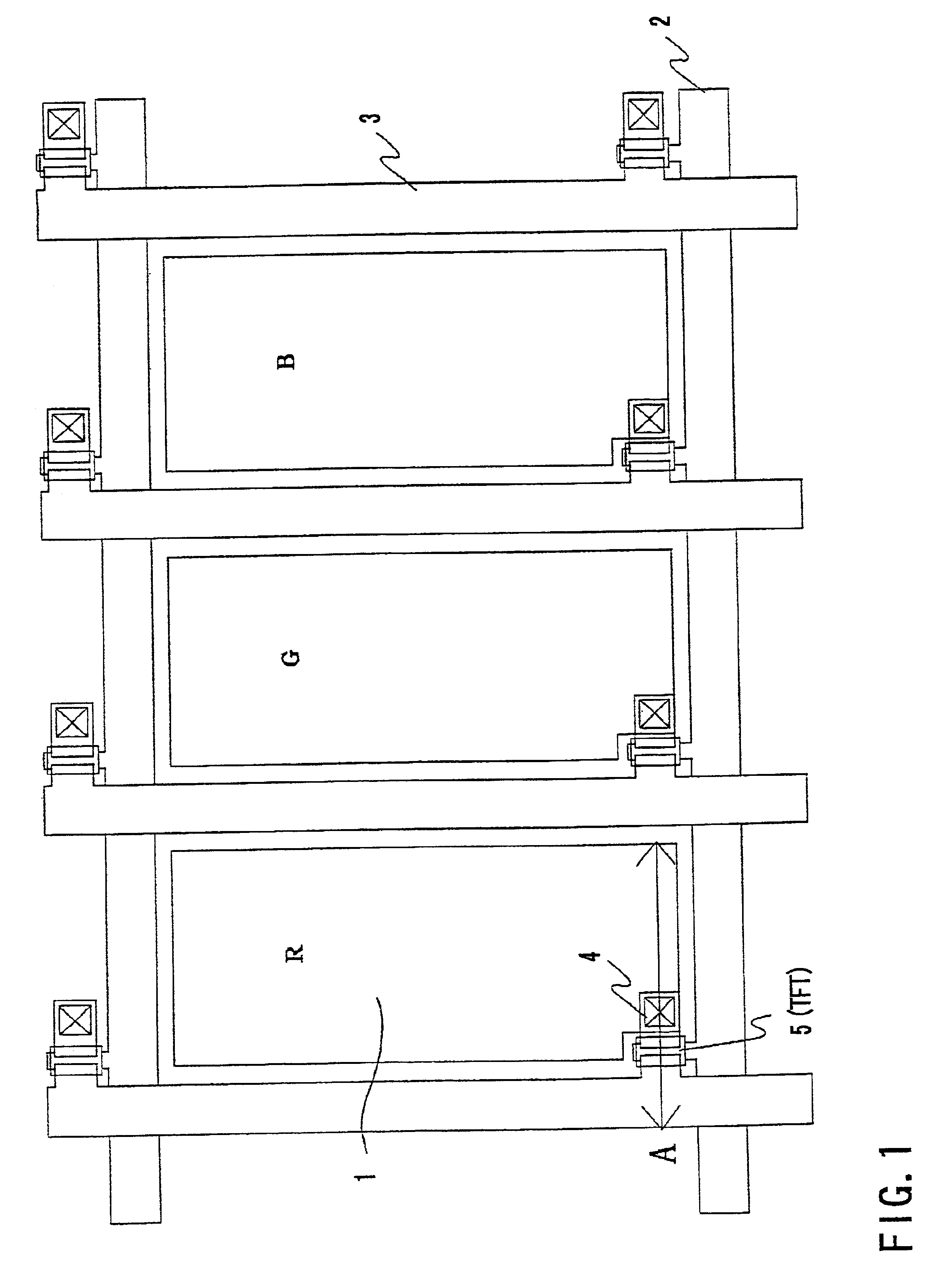
FIG. 1 is a plan view showing pixels formed on an active matrix substrate of an OCB type liquid crystal display according to the present embodiment. As shown in FIG. 1, pixel electrodes 1 are disposed in a matrix on the active matrix substrate. Also, there are disposed gate lines 2 and drain lines 3 which pass along the periphery of the pixel electrodes 1 and which are perpendicular to each other. In the proximity of each of intersections between the gate lines 2 and the drain lines 3, there is disposed a thin film transistor (TFT) 5. A drain electrode of each TFT 5 is coupled with the drain line 3, and a gate electrode of each TFT 5 is coupled with the gate line 2. Also, a source electrode of each TFT 5 is coupled with the pixel electrode 1 via a contact hole 4. By using three sets of the pixel electrodes 1 and the TFT's 5 which perform image display of red (R) color, green (G) color and blue (B) color, respectively, it becomes possible to constitute one pixel for col...

embodiment 2

[Embodiment 2]

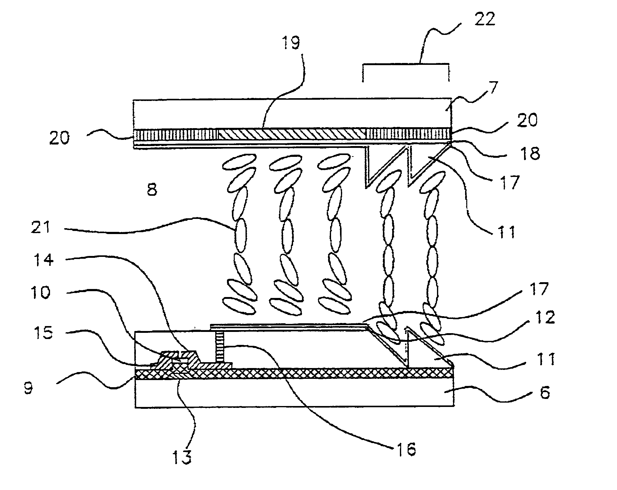
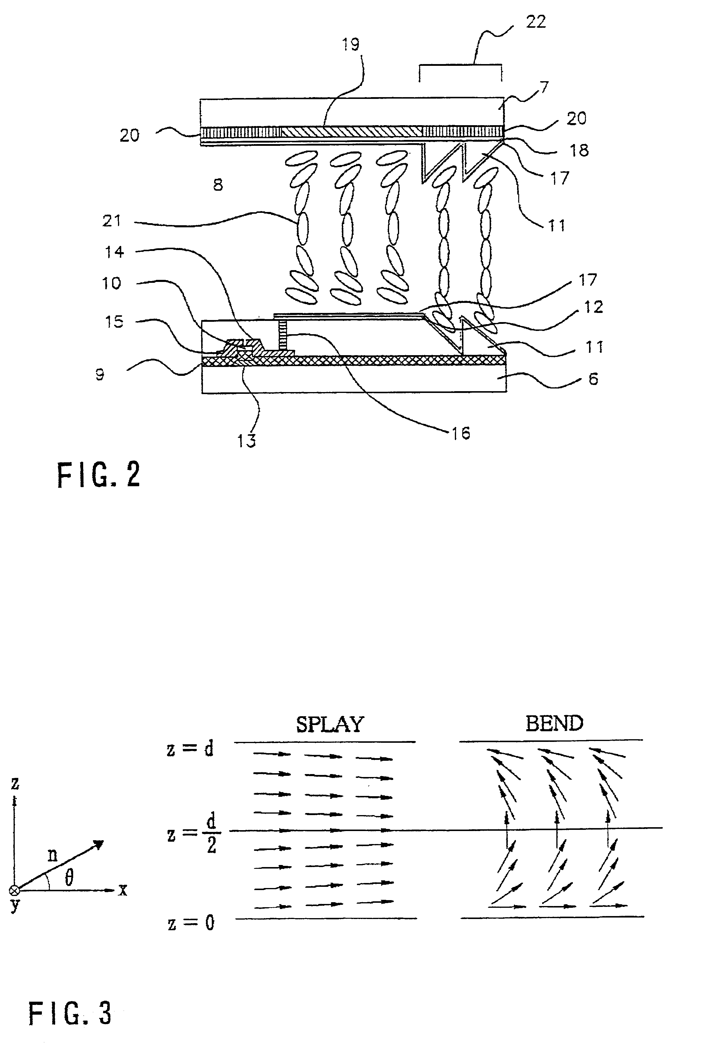
FIG. 8 is a partial schematic cross sectional view of a pixel portion of an OCB type liquid crystal display according to a second embodiment of the present invention. FIG. 8 is a cross sectional view approximately taken along the line A—A in FIG. 1. As shown in FIG. 8, the OCB type liquid crystal display according to the present embodiment comprises a lower side substrate 6, an opposing side substrate 7 which is disposed on the opposite side of the lower side substrate 6, and a liquid crystal layer 8 interposed between the lower side substrate 6 and the opposing side substrate 7. The thickness of the liquid crystal layer 8 is 5-6 μm. On the lower side substrate 6, there are disposed a gate insulating film 9, a TFT 10, an insulating film 11, a pixel electrode 12, a color filter 19 and a light shield film 20. More particularly, on the lower side substrate 6, there is stacked the gate insulating film 9 which is made of photosensitive acrylic resin. On the gate insulating ...

embodiment 3

[Embodiment 3]

With reference to FIGS. 9A-9G and FIGS. 10A-10F, an explanation will now be made on another method of manufacturing an active matrix substrate used in the OCB type liquid crystal display according to the present invention. A process for fabricating portions of the OCB type liquid crystal display other than the active matrix substrate may be the same as that described with reference to the first embodiment.

First, gate electrodes 13 are formed on a lower side substrate 6, and a gate insulating film 9 is stacked on the gate electrodes 13 and lower side substrate 6. Source electrodes 14 and drain electrodes 15 are formed on the gate insulating film 9, and thereby an active matrix substrate having TFT's 10 as switching elements is formed, as shown in FIG. 9A. Here, it should be noted that each of the switching elements is not limited to the TFT, but may be constituted of other switching element, for example, a diode and the like.

Thereafter, an insulating film 11 which is ma...


PUM

PropertyMeasurementUnit
angleaaaaaaaaaa
response timeaaaaaaaaaa

Abstract

An OCB type liquid crystal display having first and second substrates opposed to each other via a liquid crystal layer such that rubbing directions of the first and second substrates become parallel to each other, a plurality of pixel electrodes which correspond to respective pixels, and a common electrode formed on the second substrate which receives a reference voltage commonly to a plurality of the pixels. A first transition nucleus area is formed in the first substrate layer and has a plurality of continuous slant surfaces having a saw-tooth cross sectional profile, and a second transition nucleus area is formed in the second substrate and has a plurality of continuous slant surfaces having a saw-tooth cross sectional profile. The slant surfaces in the first and second transition nucleus areas oppose to each other and slope toward mutually opposite angular directions.

Description

FIELD OF THE INVENTIONThe present invention relates generally to an Optically Compensated Birefringence (OCB) type liquid crystal display, and more particularly to an OCB type liquid crystal display in which transition of liquid crystal molecules from splay alignment to bend alignment can be made easily by a low transition voltage and without deteriorating display quality.BACKGROUND OF THE INVENTIONA twisted nematic (TN) system is widely used in a liquid crystal display at present. The liquid crystal display of the TN system has a high image display contrast, but has a problem that the viewing angle dependence is large. In order to improve viewing angle characteristics of the TN type liquid crystal display, various methods have been proposed including a pixel domain division technology. However, another problem that the liquid crystal display of the TN system has a low response speed is not yet resolved. That is, a response speed of the liquid crystal display which uses nematic type...

Claims


Application Information

Patent Timeline
Patent Type & Authority Patents(United States)
IPC IPC(8): G02F1/1337G02F1/13G02F1/139G02F1/1333G02F1/1362
CPCG02F1/133753G02F1/1395G02F1/133784G02F1/136209G02F2001/133776G02F2001/133388G02F1/1393G02F1/133388G02F1/133776G02F1/1337
Inventor KONNO, TAKAYUKISUKEGAWA, OSAMUSUZUKI, MASAYOSHIWATANABE, MAKOTO
Owner VISTA PEAK VENTURES LLC
Why Eureka
Try Eureka