High-inductance-value silica-based planar spiral inductor structure

A plane spiral and inductance technology, applied in circuits, electrical components, electric solid devices, etc., can solve the problems of limited use range, large inductance volume, small inductance value, etc., to improve inductance value, reduce eddy current loss, and improve inductance. effect of value

Active Publication Date: 2013-08-14
JIANGYIN CHANGDIAN ADVANCED PACKAGING CO LTD
View PDF4 Cites 6 Cited by
  • Summary
  • Abstract
  • Description
  • Claims
  • Application Information

AI Technical Summary

Problems solved by technology

At present, this kind of power inductor is usually a separate surface mount component, but this kind of inductor is bulky and expensive
However, the planar

Method used


Image

  • High-inductance-value silica-based planar spiral inductor structure
  • High-inductance-value silica-based planar spiral inductor structure
  • High-inductance-value silica-based planar spiral inductor structure

Examples


Embodiment Construction

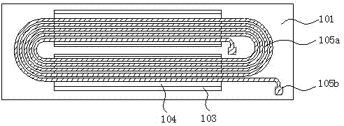
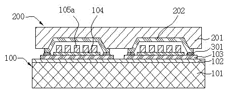
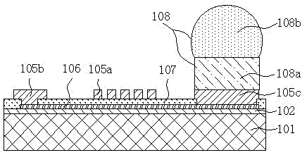
[0048] see figure 1 and figure 2 , the present invention is a high-inductance silicon-based planar spiral inductor structure, including a silicon-based planar spiral inductor 100 and a thin-film silicon cap 200 . The silicon-based planar spiral inductor 100 includes a silicon substrate 101 and a planar spiral inductor coil 105. A passivation layer 102 is deposited on the silicon substrate 101. The passivation layer 102 can be silicon dioxide, silicon nitride or other insulating properties. organic material coating, and the passivation layer 102 completely covers the upper surface of the silicon substrate 101 . The planar spiral inductance coil 105 includes an inductance coil 105a and terminals 105b arranged at both ends of the inductance coil 105a. The inductance coil 105a has a planar spiral structure, and the spiral structure can be rectangular, square, circular or other similar shapes, such as oval, and the number of turns of the inductance coil 105a is usually greater ...


PUM


Abstract

The invention relates to a high-inductance-value silica-based planar spiral inductor structure, and belongs to the technical field of semiconductor encapsulation. The structure comprises a planar spiral inductor (100) and a thin film silicon cap (200); a dielectric layer I (104), a magnetic film layer I (103), a passivation layer (102) and a silicon substrate (101) are sequentially arranged under an inductance coil (105a); a thin film silicon cap (200) provided with a magnetic film layer II (202) is covered on the planar spiral inductor (100) and connected with the planar spiral inductor (100) through an adhesive; and the magnetic film layer I (103) and/or the magnetic film layer II (202) consist(s) of a plurality of magnetic film bars perpendicular to the inductance coil. According to the invention, the magnetic film layer I, the magnetic film layer II and the adhesive form a complete magnetic return path from the center of the inductance coil to the outside, the design which is capable of reducing eddy current loss can obviously improve the inductance value, and a wafer level mode implementation process is adopted to allow the size of the planar spiral inductor to be smaller and the manufacturing cost to be lower.

Description

technical field [0001] The invention relates to a high-inductance silicon-based planar spiral inductance structure, which belongs to the technical field of semiconductor packaging. Background technique [0002] Inductors are very common passive components in circuit systems, which can perform functions such as filtering, choking, and storing energy. In power devices such as DC-DC converters (DC-DC Convertor), inductors play the role of storing energy. The amount of energy stored in an inductor is proportional to its inductance value. In order to meet the performance requirements of the power system, the inductance value of this power inductor is relatively large. At present, this power inductor is usually a separate surface mount component, but this inductor is bulky and expensive. However, the planar spiral inductor with small volume and relatively cheap manufacturing cost has a small inductance value, which limits its application range in circuit systems. Contents of t...

Claims


Application Information

Patent Timeline
IPC IPC(8): H01L23/64
CPCH01L2924/0002
Inventor 郭洪岩张黎陈锦辉赖志明
Owner JIANGYIN CHANGDIAN ADVANCED PACKAGING CO LTD
Why Eureka
Try Eureka