LED flip chip and manufacturing method thereof

A technology of flip chip and manufacturing method, which is applied in the direction of electrical components, electric solid devices, circuits, etc., can solve problems such as LED chip failure and LED chip short circuit, and achieve the effect of increasing the welding area and reducing precision requirements

Inactive Publication Date: 2013-08-14
ELEC TECH PHOTOELECTRIC TECH DALIAN
View PDF5 Cites 9 Cited by
  • Summary
  • Abstract
  • Description
  • Claims
  • Application Information

AI Technical Summary

Problems solved by technology

[0008] see image 3 At the same time, in the flip-chip LED chip, the heat generated by the PN junction is mainly transferred to the heat-conducting substrate 82 or the outside world through the metal bumps 78, 79, because the thickness of the epitaxial structure of the flip-chip is only a few microns and it is compatible with the solder layer used for welding. 81 is close to each other. During the process of fixing the flip-c

Method used


Image

  • LED flip chip and manufacturing method thereof
  • LED flip chip and manufacturing method thereof
  • LED flip chip and manufacturing method thereof

Examples


Embodiment Construction

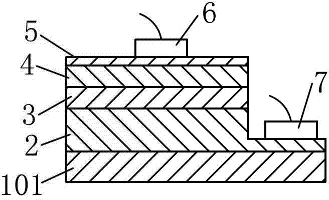
[0040] see Figure 4 and Figure 5 , LED flip-chip, including a sapphire substrate 1, sequentially arranged on the sapphire substrate 1 from bottom to top, and sequentially provided with an N-type layer 11, a light-emitting layer 12, a P-type layer 13, a reflective layer 15, The first insulating layer 16 . The first insulating layer 16 is provided with an N lead electrode 17 and a P lead electrode 18, and the N lead electrode 17 extends from the P-type layer 13 to the hole 14 of the N-type layer 11 along the depth (refer to Figure 9 ) is electrically connected to the N-type layer 11 , and the P lead electrode 18 is electrically connected to the reflective layer 15 . The N lead electrode 17 and the P lead electrode 18 are provided with a second insulating layer 22 , and the second insulating layer 22 is provided with a through hole 28 . The N pad layer 26 and the P pad layer 27 are respectively disposed on the second insulating layer 22 , and respectively contact the N lead e...


PUM


Abstract

The invention provides an LED (light emitting diode) flip chip which comprises a sapphire substrate, an N-shaped layer, a light emitting layer, a P-shaped layer, a reflecting layer, a first insulating layer, an N bonding pad layer and a P bonding pad layer, wherein the N-shaped layer, the light emitting layer, the P-shaped layer, the reflecting layer and the first insulating layer are arranged on the sapphire substrate in sequence from bottom to up; N leading wire electrodes and P leading wire electrodes are arranged on the first insulating layer; the N leading wire electrodes are conductively connected with the N-shaped layer; the P leading wire electrodes are in conductively connected with the reflecting layer; the N bonding pad layer is conductively connected with the N leading wire electrodes; the P bonding pad layer is conductively connected with the P leading wire electrodes; a second insulating layer is arranged on the N leading wire electrodes and the P leading wire electrodes; through holes are formed in the second insulating layer; and the N bonding pad layer and the P bonding pad layer are in contact with the N leading wire electrodes and the P leading wire electrodes through the through holes respectively. The LED flip chip and the manufacturing method thereof are beneficial to heat radiation of the LED flip chip, enable the LED flip chip to have a favorable insulating effect, and improve the stability of the LED flip chip.

Description

technical field [0001] The invention relates to the technical field of LEDs, in particular to an LED flip chip and a manufacturing method thereof. Background technique [0002] The structure of a traditional GaN-based LED chip on a sapphire substrate is as follows: figure 1 As shown, an N-type GaN layer 2, a quantum well QW active region 3, a P-type GaN layer 4, and a current spreading layer 5 are sequentially arranged on the substrate 101 from bottom to top, and on the current spreading layer 5 and the N-type GaN layer P electrodes 6 and N electrodes 7 are arranged in distribution. In this structure, the P electrode 6 is just located on the light-emitting surface of the chip; at the same time, a small part of the P-type GaN layer 4 and the quantum well QW active region 3 are etched, so that the N-electrode 7 forms an electrical connection with the N-type GaN layer 2 below. touch. Light is taken out from the upper P-type GaN layer 4 , and the limited electrical conductivi...

Claims


Application Information

Patent Timeline
IPC IPC(8): H01L33/48H01L33/62
CPCH01L2224/14H01L2224/49107
Inventor 王冬雷莫庆伟
Owner ELEC TECH PHOTOELECTRIC TECH DALIAN
Why Eureka
Try Eureka