Pixel circuit and driving method thereof

A pixel circuit and circuit technology, applied in static indicators, instruments, etc., can solve the problems of uneven film thickness and non-uniform electrical performance of light-emitting devices, and achieve the goal of eliminating uneven film thickness, improving quality, and improving compensation effects Effect

Active Publication Date: 2013-08-21
BOE TECH GRP CO LTD
View PDF5 Cites 10 Cited by
  • Summary
  • Abstract
  • Description
  • Claims
  • Application Information

AI Technical Summary

Problems solved by technology

[0006] Third, the uneven film thickness of the light-emitting device will also cause non-uniformity in electrical properties during evaporation

Method used


Image

  • Pixel circuit and driving method thereof
  • Pixel circuit and driving method thereof
  • Pixel circuit and driving method thereof

Examples


Embodiment 1

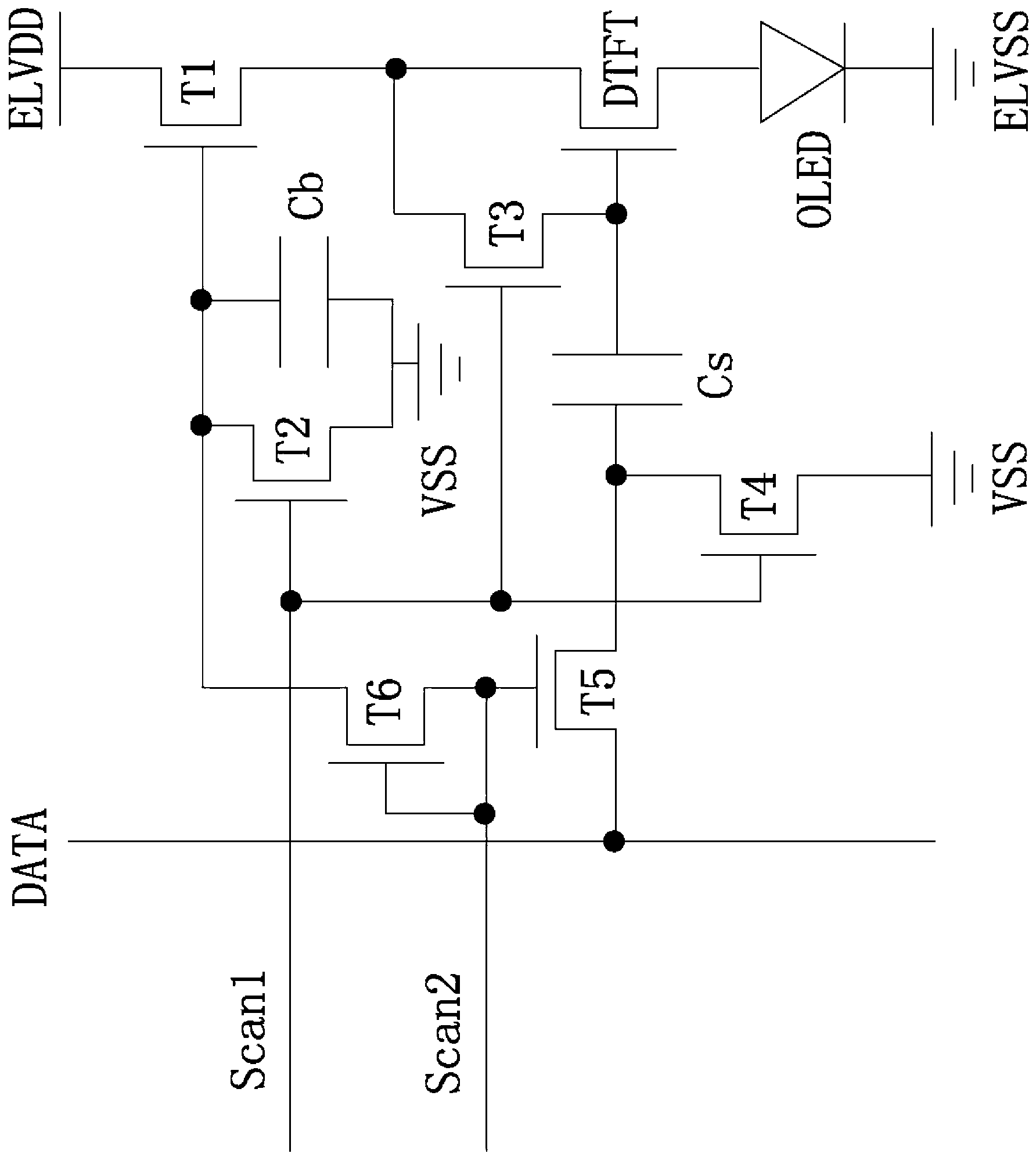
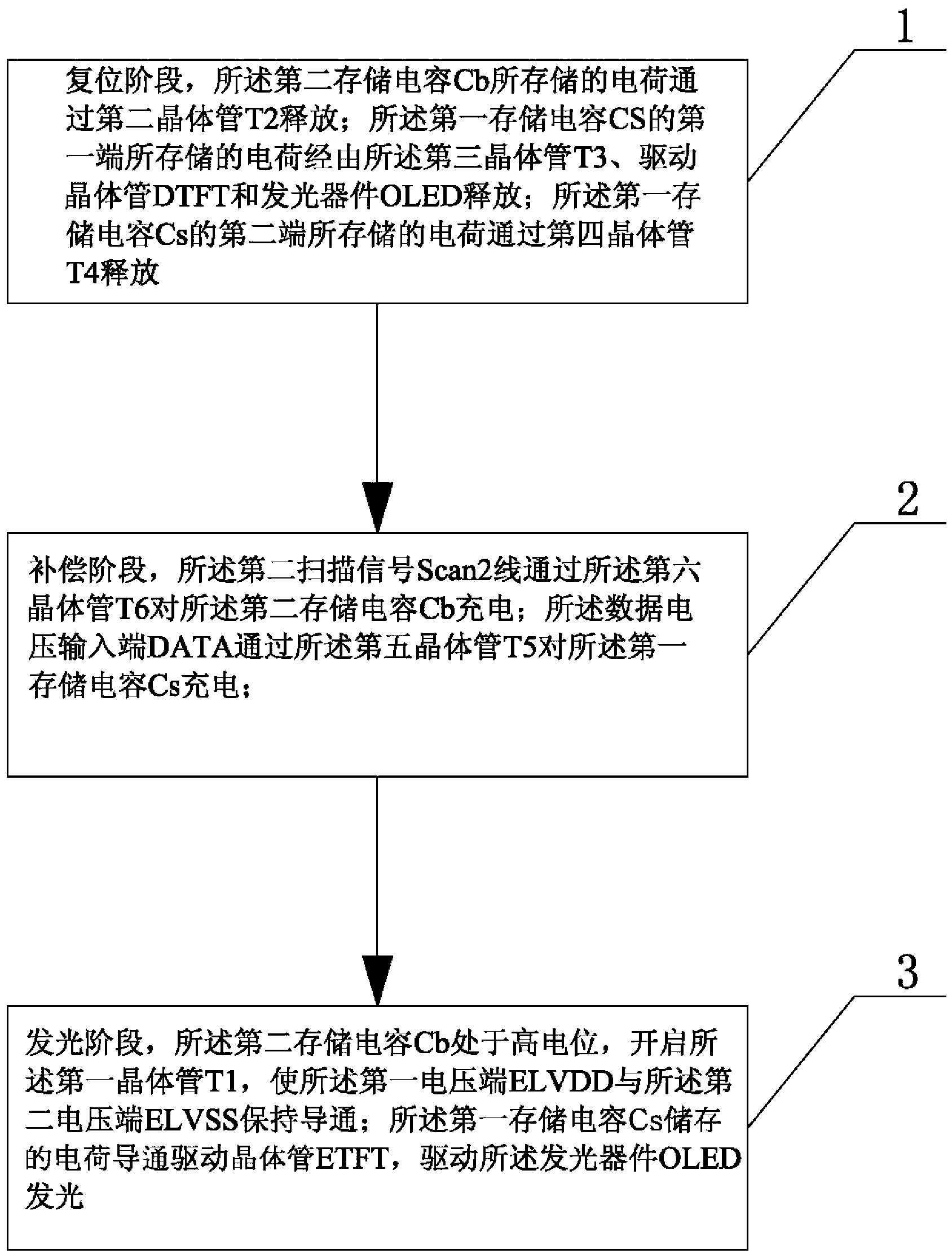
[0042] see figure 1 As shown, the pixel circuit described in the embodiment of the present invention is mainly used for the driving compensation of each light-emitting device in the active matrix light-emitting organic electric display tube. Each light-emitting device is driven and compensated by a pixel circuit, and each pixel circuit includes: Subcircuits, charging subcircuits, driving subcircuits and light emitting devices; wherein,

[0043] The first terminal of the light emitting device OLED is connected to the second voltage terminal ELVSS;

[0044] The driving sub-circuit includes a driving transistor DTFT, a first transistor T1, a third transistor T3, a first storage capacitor Cs, and a second storage capacitor Cb, and the source of the driving transistor DTFT is connected to the drain of the first transistor T1 and the drain of the third transistor T3, the drain of the driving transistor DTFT is connected to the second terminal of the light emitting device OLED, the ...

Embodiment 2

[0067] The pixel circuit and driving method in this embodiment are improvements on the basis of Embodiment 1. The technical content disclosed in Embodiment 1 will not be described repeatedly, and the content disclosed in Embodiment 1 also belongs to the content disclosed in this embodiment.

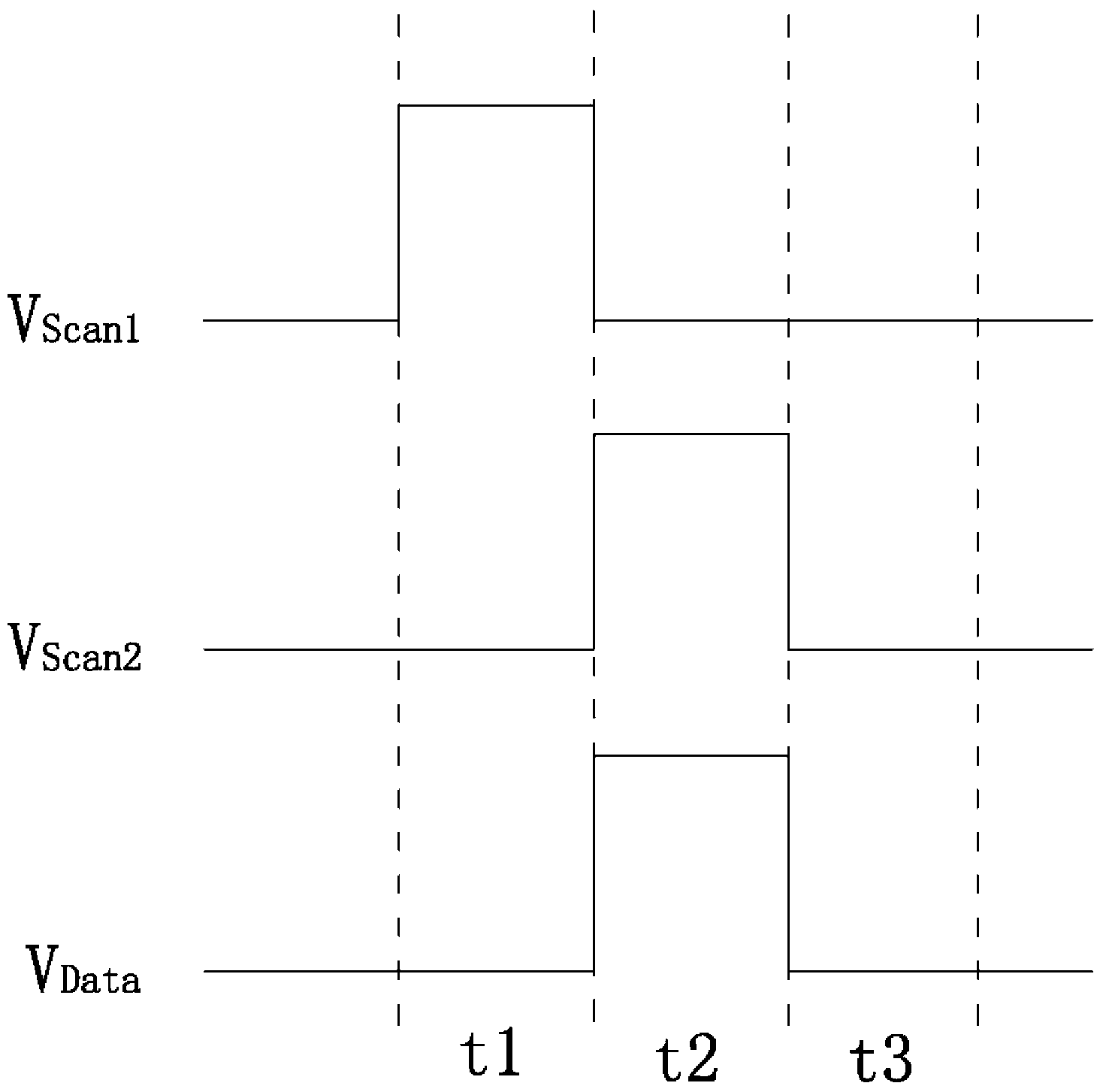
[0068] see Figure 4 As shown, as a modified technical solution of the technical solution in Embodiment 1; the pixel circuit also includes a third scanning signal line Scan3; specifically: the charging sub-circuit includes a fifth transistor T5 and a sixth transistor T6, so The source of the fifth transistor T5 is connected to the data voltage input terminal DATA, the drain of the fifth transistor T5 is connected to the source of the fourth transistor T4, and the gate of the fifth transistor T5 is connected to the second scanning signal line Scan2; the gate of the sixth transistor T6 and the source of the sixth transistor T6 are connected to the third scanning signal line Scan3, and the d...


PUM


Abstract

The invention relates to the technical field of displaying, in particular to a pixel circuit and a driving method thereof. The pixel circuit comprises a driving sub circuit, a resetting sub circuit and a charging sub circuit. The driving sub circuit comprises a driving transistor, a first transistor, a third transistor, a first memory capacitor and a second memory capacitor. The resetting sub circuit is used for conducting discharging on the first memory capacitor and the second memory capacitor under the control of a first scanning signal output by a first scanning signal line. The charging sub circuit comprises a fifth transistor and a sixth transistor. According to the pixel circuit, nonuniformity caused by the threshold voltage of the transistors and the phenomenon of image retention caused by threshold voltage drift can be effectively removed through compensation, and the problem of uneven brightness of an active matrix light-emitting organic electroluminescent display tube due to the fact that the threshold voltages of the driving transistors between light-emitting devices of different pixel cells are different in the active matrix light-emitting organic electroluminescent display tube is solved.

Description

technical field [0001] The present invention relates to the field of display technology, in particular to a pixel circuit and a driving method thereof. Background technique [0002] Organic Light-Emitting Diode (OLED, Organic Light-Emitting Diode), as a current-mode light-emitting device, has been increasingly used in high-performance active-matrix light-emitting organic electroluminescent display tubes. Traditional passive matrix organic electroluminescent display tubes (Passive Matrix OLED) require shorter driving time of a single pixel with the increase of display size, thus need to increase transient current and increase power consumption. At the same time, the application of high current will cause the voltage drop on the nano-indium tin metal oxide line to be too large, and the working voltage of the OLED will be too high, thereby reducing its efficiency. The active matrix organic electroluminescent display tube (AMOLED, Active Matrix OLED) scans input OLED current ro...

Claims


Application Information

Patent Timeline
Patent Type & Authority Applications(China)
IPC IPC(8): G09G3/32
CPCG09G3/3233G09G2300/0819G09G2300/0852G09G2300/0861G09G2320/0233G09G2320/043G09G2310/0251G09G3/3225G09G3/3291G09G2300/0809G09G2300/0876G09G2320/0257
Inventor 杨飞
Owner BOE TECH GRP CO LTD
Why Eureka
Try Eureka