A kind of preparation method of near-infrared photoelectric silicon material

A near-infrared optical and electrical material technology, which is applied in the preparation of near-infrared optoelectronic materials, can solve the problems of affecting optoelectronic properties and the decrease of sulfur ion concentration, and achieves the effect of high near-infrared absorption coefficient

Inactive Publication Date: 2015-11-18
SOUTH CHINA NORMAL UNIVERSITY
View PDF8 Cites 0 Cited by
  • Summary
  • Abstract
  • Description
  • Claims
  • Application Information

AI Technical Summary

Problems solved by technology

[0004] The laser-assisted doping method is superior to the ion implantation method, but during the annealing process, sulfur ions will slowly precipitate out of the silicon surface layer, resulting in a decrease in the concentration of sulfur ions in the laser-doped layer, affecting its photoelectric performance

Method used


Image

  • A kind of preparation method of near-infrared photoelectric silicon material
  • A kind of preparation method of near-infrared photoelectric silicon material
  • A kind of preparation method of near-infrared photoelectric silicon material

Examples


Embodiment 1

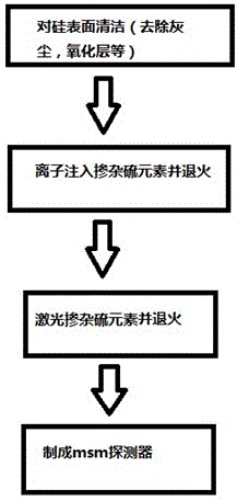
[0031] Such as figure 1 As shown in, the preparation method of the near-infrared photoelectric silicon material provided in this embodiment includes the following steps:

[0032] (1) Clean the surface of the single crystal silicon. The cleaning process includes placing the silicon in an acetone solution, placing the acetone solution soaked with the silicon wafer in the ultrasonic chamber, turning on the switch of the ultrasonic chamber, and taking out the cleaned silicon after 20 minutes. slice, and load it on the stage of the vacuum chamber;

[0033] (2) Perform heavy sulfur doping on the crystalline silicon wafer, vacuumize the vacuum chamber, and adjust the pressure to 1×10 -3 Below Pa, open the inflation valve and flush into the background gas SF at a flow rate of 40 sccm 6 , until the pressure in the vacuum chamber is 0.5±0.01pa, after the pressure in the vacuum chamber is stable, turn on the femtosecond (or nanosecond) laser and adjust the laser intensity to 1.8J / cm 2...

Embodiment 2

[0039] like figure 1 As shown in, the preparation method of the near-infrared photoelectric silicon material provided in this embodiment includes the following steps:

[0040] (1) Clean the surface of monocrystalline silicon. The cleaning process includes placing the silicon in acetone solution for several minutes, placing the acetone solution soaked with silicon wafers in the ultrasonic chamber, turning on the switch of the ultrasonic chamber, and taking it out for 20 minutes to complete the cleaning. The silicon wafer is loaded on the stage of the vacuum chamber;

[0041] (2) Perform heavy sulfur doping on the crystalline silicon wafer, vacuumize the vacuum chamber, and adjust the pressure to 1×10 -3 Below Pa, open the inflation valve and flush into the background gas SF at a flow rate of 40 sccm 6 , until the pressure in the vacuum chamber is 0.5±0.01pa, after the pressure in the vacuum chamber is stable, turn on the femtosecond (or nanosecond) laser and adjust the laser in...


PUM


Abstract

The invention discloses a method for preparing near-infrared light electrical silicon materials. The method comprises a step of mingling sulphur to a crystal silicon wafer in a heavy doping mode, and a step of placing the crystal silicon wafer which is mingled with the sulphur in the heavy doping mode to an annealing device, wherein an electric field auxiliary annealing method is adopted, the voltage of the annealing electric field cannot break through the silicon wafer, the temperature of annealing is 550 DEG C, and the annealing process takes 6 hours. The method can keep the sulphur which is mingled into the crystal silicon wafer from being separated out in the process of annealing, the sulphur in a sulphur layer which is mingled into the crystal silicon wafer surface in the heavy doping mode keeps high concentration, and the photoelectric property of the near-infrared light silicon materials can be improved.

Description

technical field [0001] The invention belongs to the technical field of crystalline silicon, and in particular relates to a preparation method of a near-infrared photoelectric material. Background technique [0002] Heavily doped sulfur silicon material (sulfurhypedopedsilicon) is considered to be a material capable of forming an intermediate band impurity level, and its research begins with the study of black silicon. The study found that the physical source of the light absorption of black silicon whose energy in the near-infrared part is smaller than the forbidden band width is the heavy doping of sulfur. Silicon is heavily doped with sulfur, and the material undergoes a Mott phase transition, which significantly improves the absorption of silicon materials in the infrared part. Therefore, heavily doped sulfur silicon materials have very important application potential in photovoltaic cells, communication sensors and other fields. [0003] At present, in the prior art, m...

Claims


Application Information

Patent Timeline
Patent Type & Authority Patents(China)
IPC IPC(8): H01L21/324
Inventor 陈长水
Owner SOUTH CHINA NORMAL UNIVERSITY
Why Eureka
Try Eureka