Refracting high-power semiconductor laser array beam shaping device

A laser array and laser beam technology, applied in the field of laser technology applications, can solve the problems of difficult processing, difficult assembly adjustment, low precision, etc., and achieve the effects of low processing difficulty, high shaping efficiency, and reduced focal length

Active Publication Date: 2013-09-04
XI'AN INST OF OPTICS & FINE MECHANICS - CHINESE ACAD OF SCI
View PDF5 Cites 5 Cited by
  • Summary
  • Abstract
  • Description
  • Claims
  • Application Information

AI Technical Summary

Problems solved by technology

[0012] In order to overcome the shortcomings of difficult processing, serious error accumulation, difficult assembly and adjustment, and low precision in the above scheme, the present invention provides an optical shaping device for high-power semiconductor laser arrays, which can shape the beam while realizing beam shaping The thickness of each step glass in the component is doubled, and the accumulation of errors is reduced by half, which greatly reduces the difficulty of processing, improves the accuracy and reduces loss, and at the same time compresses the width of the laser beam in the fast axis direction and reduces the focal length of the focusing lens. make the system more compact

Method used


Image

  • Refracting high-power semiconductor laser array beam shaping device
  • Refracting high-power semiconductor laser array beam shaping device
  • Refracting high-power semiconductor laser array beam shaping device

Examples


Embodiment 1

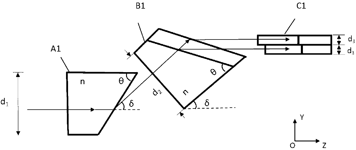
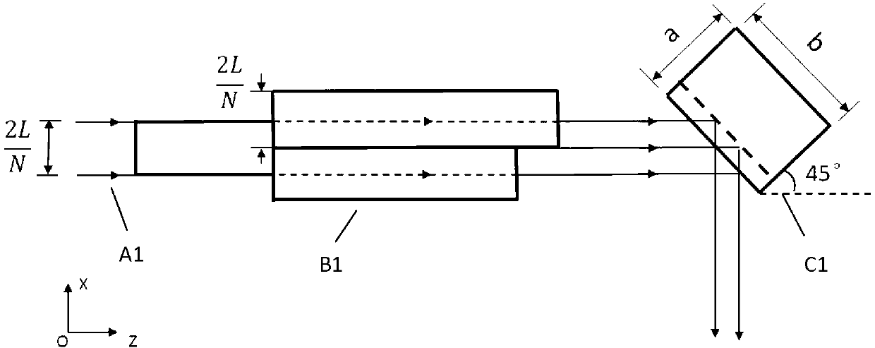
[0049] In this embodiment, the light beam emitted by the one-dimensional array of semiconductor lasers is divided into N equal parts in the direction of the slow axis, where N=2K (K is a natural number), and N is obtained according to the product relationship between the optical parameters of the fast axis and the slow axis, its satisfying relationship BPP in the equation f and BPP S are the fast-axis and slow-axis optical parameter products calculated after the one-dimensional array beam is collimated, respectively. Assuming N=6, see Figure 9 The structure of the shaping system in this embodiment includes a semiconductor laser one-dimensional array light source 1, a fast-axis collimator lens 2, a slow-axis collimator lens 3, the first right-angle transmission trapezoidal glass group A, and the second right-angle transmission trapezoidal glass group B and rectangular reflective glass set C.

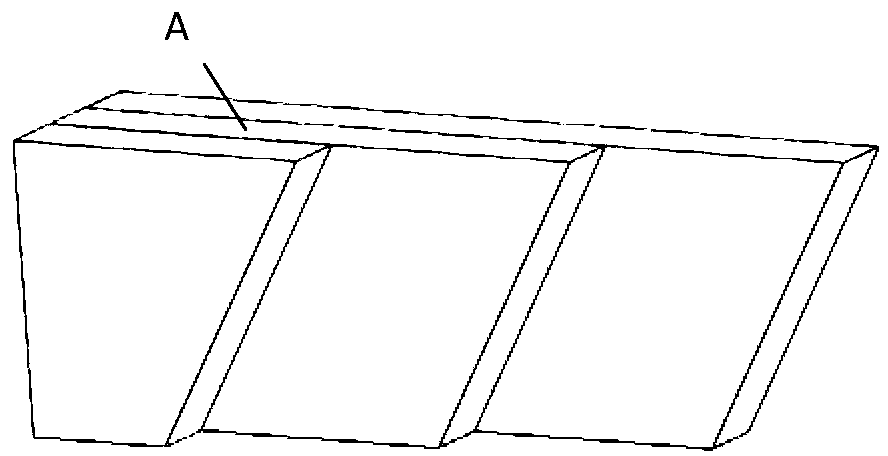
[0050] The first right-angled trapezoidal transmission glass group A is compose...

Embodiment 2

[0059] In this embodiment, the light beams emitted by the two-dimensional array of semiconductor lasers are collimated along the fast and slow axes and compressed along the fast axes to form elongated light spots, and then undergo beam shaping by the shaping device. refer to Figure 11 , specifically, the light emitted by the semiconductor laser two-dimensional array 8 passes through the fast-axis collimating cylindrical lens 9 and the slow-axis collimating microlens array 10 in turn, and then passes through the first right-angle trapezoidal glass group A and the second right-angled trapezoidal glass group A. Group B, beam shaping device composed of rectangular glass group C.

[0060] In this embodiment, assuming that the number of cuts of the two-dimensional beam along the slow axis direction is N=6, the beam width H in the fast axis direction after the two-dimensional beam is collimated and compressed in the fast axis direction, the two-dimensional beam in the slow axis dire...


PUM


Abstract

The invention provides a refracting high-power semiconductor laser array beam shaping device. While a beam is shaped, the thickness size of each block of step glass in a shaping element can be doubled, the error accumulation can be reduce by half, the processing difficulty is greatly reduced, the precision is improved, the loss is reduced, meanwhile, the width of a laser beam in the direction of a quick axis is compressed, the focal distance of a focusing lens is reduced, and a system is more compact. When a plurality of bars and a laminated array optical fiber are coupled and cutting number is relatively large, the advantages of the element can be better embodied.

Description

technical field [0001] This patent relates to a beam shaping device for a high-power semiconductor laser array, which belongs to the scope of the application field of laser technology. Background technique [0002] Due to the advantages of small size, high photoelectric conversion efficiency, long working life, and low cost, semiconductor lasers are widely used in material processing, laser medical treatment, and pump sources for solid-state lasers. [0003] However, compared with other lasers, the biggest defect of semiconductor lasers is that the beam quality is poor. The use of conventional lenses and optical systems to couple light beams into optical fibers seriously restricts the development of semiconductor lasers. In order to make the beam emitted by the semiconductor laser can be smoothly coupled into the optical fiber, the beam must be collimated and beam transformed and shaped. [0004] Semiconductor laser arrays are divided into one-dimensional arrays and two-di...

Claims


Application Information

Patent Timeline
Patent Type & Authority Applications(China)
IPC IPC(8): G02B27/09
Inventor 黄志华刘兴胜熊玲玲张普王贞福刘晖
Owner XI'AN INST OF OPTICS & FINE MECHANICS - CHINESE ACAD OF SCI
Why Eureka
Try Eureka