Shifting register, array substrate and display panel

A technology of shift register and shift register circuit, which is applied in static memory, digital memory information, instruments, etc., and can solve the problems of inability to test display panels, inability to measure RGB DC pure color images well, and inability to comprehensively measure display panels Performance and other issues, to achieve the effect of improving the factory yield and distinguishing bad

Active Publication Date: 2013-09-11
SHANGHAI AVIC OPTOELECTRONICS
View PDF4 Cites 6 Cited by
  • Summary
  • Abstract
  • Description
  • Claims
  • Application Information

AI Technical Summary

Problems solved by technology

However, because the structure of the existing shift register works in a shift register mode, the charging signal output by the previous shift register circuit is the start signal of the next shift register circuit, so the shift register can only The gate lines (Gate lines) of the display panel are charged line by line, instead of being able to charge the gate lines of al

Method used


Image

  • Shifting register, array substrate and display panel
  • Shifting register, array substrate and display panel
  • Shifting register, array substrate and display panel

Examples


Embodiment Construction

[0046] In order to make the content of the present invention clearer and easier to understand, the content of the present invention will be further described below in conjunction with the accompanying drawings. Of course, the present invention is not limited to this specific embodiment, and general replacements known to those skilled in the art are also covered within the protection scope of the present invention.

[0047] Secondly, the present invention is described in detail by means of schematic diagrams. When describing the examples of the present invention in detail, for the convenience of explanation, the schematic diagrams are not partially enlarged according to the general scale, which should not be used as a limitation of the present invention.

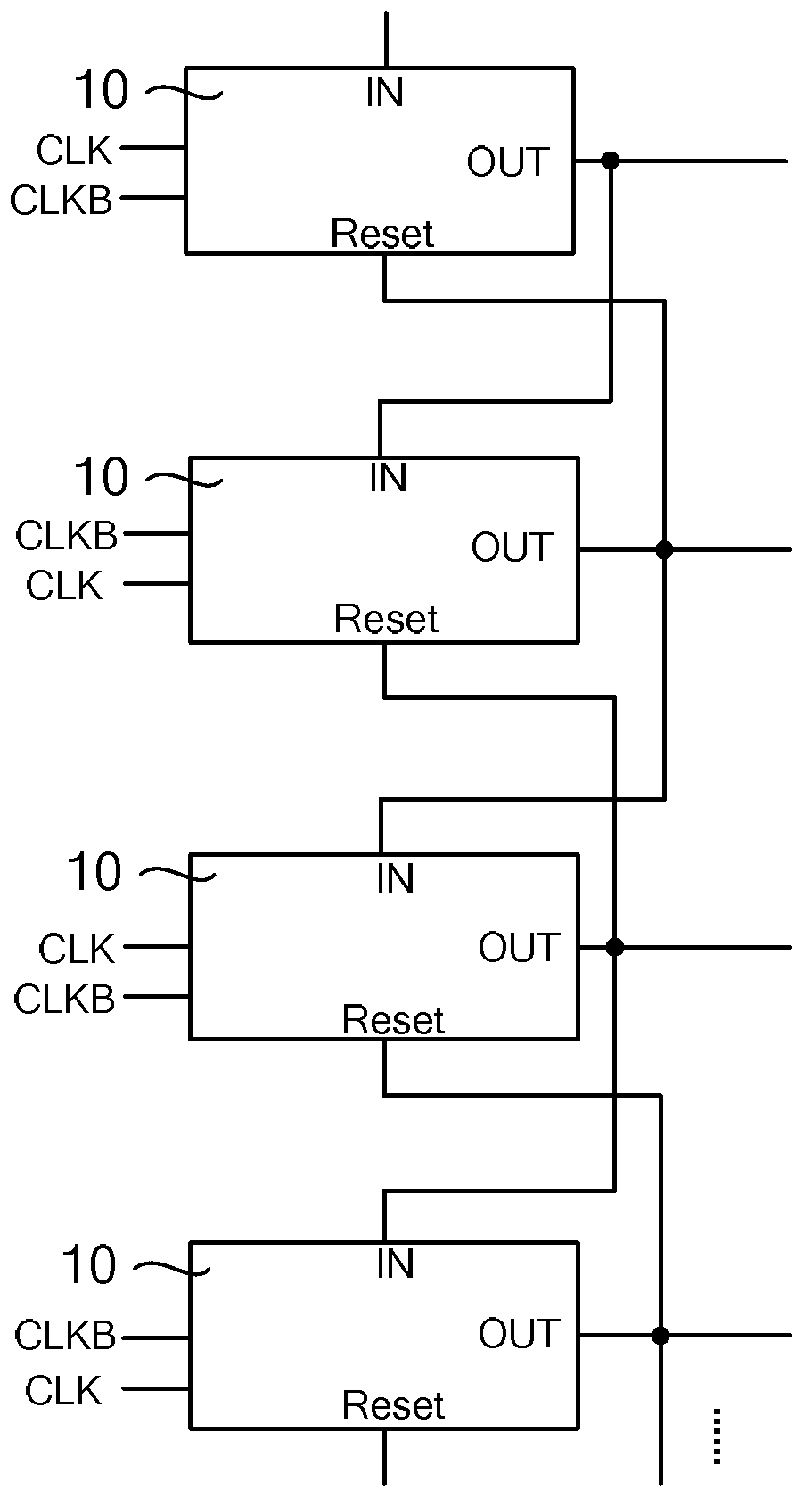
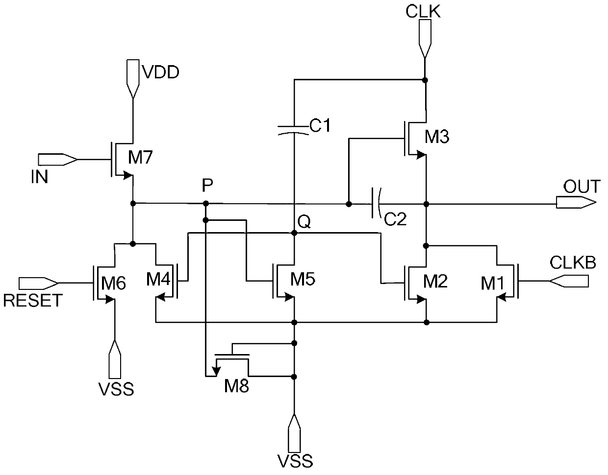
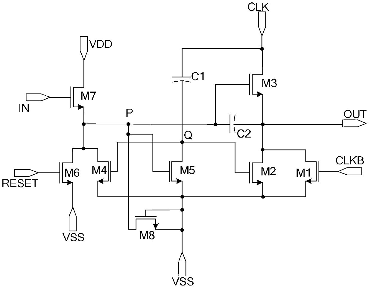
[0048] The present invention provides a shift register, including multi-stage cascaded shift register circuits, each stage of register circuits includes an open circuit, a pull-up circuit, a pull-down circuit, and a main input...


PUM


Abstract

The invention provides a shifting register, an array substrate and a display panel. The shifting register comprises multiple stages of cascade shifting registering circuits, wherein each stage of shifting registering circuit comprises a testing circuit, one end of the testing circuit is connected to a second level end in a coupled mode, the second level end outputs a high level when the shifting register is in a testing mode, and therefore the testing circuit charges the main output end. The array substrate comprises a drive circuit which is composed of the shifting register. The display panel comprises the array substrate and a color-film substrate which is opposite to the array substrate. The shifting register enables all scanning lines of the display panel to be provided with the high level simultaneously, so that direct-current pure-color image detection can be conducted on the display panel, and a traditional liquid crystal cell test is realized. Therefore, a fault caused by an array process and a fault caused by a cell process can be distinguished. In addition, a testing structure is simple, the area of an original shifting register is hardly increased and the manufacturing cost is saved.

Description

technical field [0001] The invention relates to liquid crystal flat panel display technology, in particular to a shift register, an array substrate and a display panel. Background technique [0002] The FPD (Flat Panel Display Device) technology represented by TFT-LCD (Thin film transistor-Liquid crystal display) has developed rapidly since the 1990s and gradually matured. Since TFT-LCD has the advantages of high definition, low power consumption, thinness, and portability, it has been widely used in the above-mentioned information display products, making LCD enter a new stage of high-quality, high-color display, and has broad market prospects. At present, almost all high-end LCDs use TFT active matrix without exception. TFT (Thin film transistor) active matrix mainly includes A-Si (amorphous silicon, amorphous silicon) TFT active matrix and P-Si (poly-silicon, polycrystalline silicon) TFT active matrix. Compared with P-Si TFT technology, A-Si TFT technology is more matur...

Claims


Application Information

Patent Timeline
IPC IPC(8): G09G3/20G09G3/36G11C19/28
Inventor 夏志强汪锐
Owner SHANGHAI AVIC OPTOELECTRONICS
Why Eureka
Try Eureka