Processing method of device wafer with bump

一种加工方法、器件的技术,应用在半导体/固态器件制造、电气元件、电路等方向,能够解决晶片破损、粘接剂完全除去困难等问题,达到防止破损的效果

Active Publication Date: 2013-09-11
DISCO CORP
View PDF7 Cites 10 Cited by
  • Summary
  • Abstract
  • Description
  • Claims
  • Application Information

AI Technical Summary

Problems solved by technology

[0006] However, a device wafer with bumps having a plurality of bumps formed on the surface of the semiconductor wafer has a problem that the adhesive enters the concavo-convex portions formed by the bumps, and after the device is peeled off from the carrier wafer, the intruded adhesive is removed. It is very difficult to completely remove the adhesive with fine unevenness
[0008] Therefore, when the wafer is held on the holding table and the back surface of the wafer is ground to make the wafer thinner, if the remaining area of ​​the outer periphery is not held from the lower side, the remaining area of ​​the outer periphery will be in a state of floating from the holding table, so there is a possibility of wafer damage.

Method used


Image

  • Processing method of device wafer with bump
  • Processing method of device wafer with bump
  • Processing method of device wafer with bump

Examples


Embodiment Construction

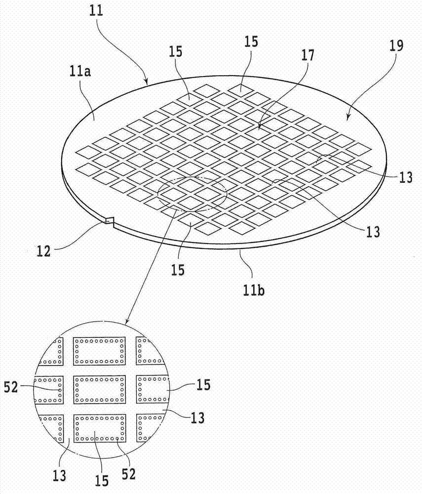
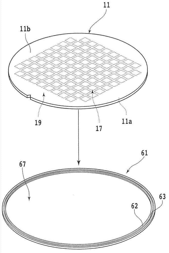
[0043] Hereinafter, embodiments of the present invention will be described in detail with reference to the drawings. figure 1 The shown device wafer 11 (hereinafter also simply referred to as "wafer 11") is formed of, for example, a silicon wafer with a thickness of 700 μm, and a plurality of dividing lines (streets) 13 are formed in a grid pattern on the surface 11a, and, Devices 15 are respectively formed in a plurality of regions divided by the plurality of planned dividing lines 13 .

[0044] Wafer 11 configured in this way includes device region 17 in which device 15 is formed and peripheral remaining region 19 surrounding device region 17 . Notches 12 are formed on the outer periphery of the wafer 11 as marks indicating the crystal orientation of the silicon wafer.

[0045] And, if figure 1 As shown in the enlarged view of , a plurality of protruding (spherical) bumps 52 are formed on four sides of each device 15 . The bumps 52 are configured to protrude from the surf...


PUM


Abstract

The invention provides a processing method of a device wafer with a bump. According to the invention, even the device wafer with the bump can be thinned and not damaged, and the devices will not be disqualified because of adhesion of the adhesive onto concave and convex parts formed by the bump. The processing method for a bump-included device wafer is characterized by including wafer so that the adhesive projects from the upper surface of an annular projection of the carrier wafer; a wafer attaching step of attaching and fixing the front side of the device wafer through the adhesive to the front side of the carrier wafer so as to accommodate bumps in a recess of the carrier wafer after performing the adhesive providing step; and a thickness reducing step of grinding or polishing the back side of the device wafer to reduce the thickness of the device wafer to a predetermined thickness after performing the wafer attaching step.

Description

technical field [0001] The present invention relates to a processing method of a semiconductor device wafer, and more specifically, relates to a technique for facilitating handling of a thinned semiconductor device wafer. Background technique [0002] In processing a wafer having a plurality of devices on its surface, such as a semiconductor device wafer or an optical device wafer, for example, backside grinding of the wafer is performed to reduce the thickness of the wafer to 50 μm or less. [0003] Handling (handling) of wafers having a thickness of 50 μm or less becomes very difficult compared with thicker wafers. Problems such as cracks occurring on the outer periphery of the wafer or a significant reduction in rigidity arise. [0004] Therefore, the following technology is known: in the state where the surface (device surface) of the wafer is attached to a carrier wafer (also referred to as a support wafer or a support plate) made of glass or silicon by using an adhesi...

Claims


Application Information

Patent Timeline
Patent Type & Authority Applications(China)
IPC IPC(8): H01L21/683H01L21/687
CPCH01L21/67092H01L21/304
Inventor D·马丁M·布朗
Owner DISCO CORP
Why Eureka
Try Eureka