
Cutting method for chip scale package glass

A glass wafer and cutting method technology, applied in the field of glass wafer cutting, can solve problems such as reducing production efficiency, affecting product quality, and black film falling off, so as to improve yield, improve cutting ability and service life, and shorten time Effect

Active Publication Date: 2013-09-18
SHENZHEN STS MICROELECTRONICS CO LTD
View PDF6 Cites 13 Cited by
  • Summary
  • Abstract
  • Description
  • Claims
  • Application Information

AI Technical Summary

Problems solved by technology

In occasions that require high edge chipping control, for example, when cutting a glass wafer with a black film attached, it is difficult to avoid the problem that the black film falls off and remains on the blue film after cutting with the traditional method, and during the peeling process Under the influence of the stress of the glass wafer, it is easy to have the problem of edge chipping on the back of the glass wafer. The occurrence of these problems will inevitably increase the packaging production time, reduce the production efficiency, seriously affect the product quality, and cause the appearance inspection product surface yield to be low

Method used


Image

  • Cutting method for chip scale package glass
  • Cutting method for chip scale package glass
  • Cutting method for chip scale package glass

Examples


Embodiment Construction

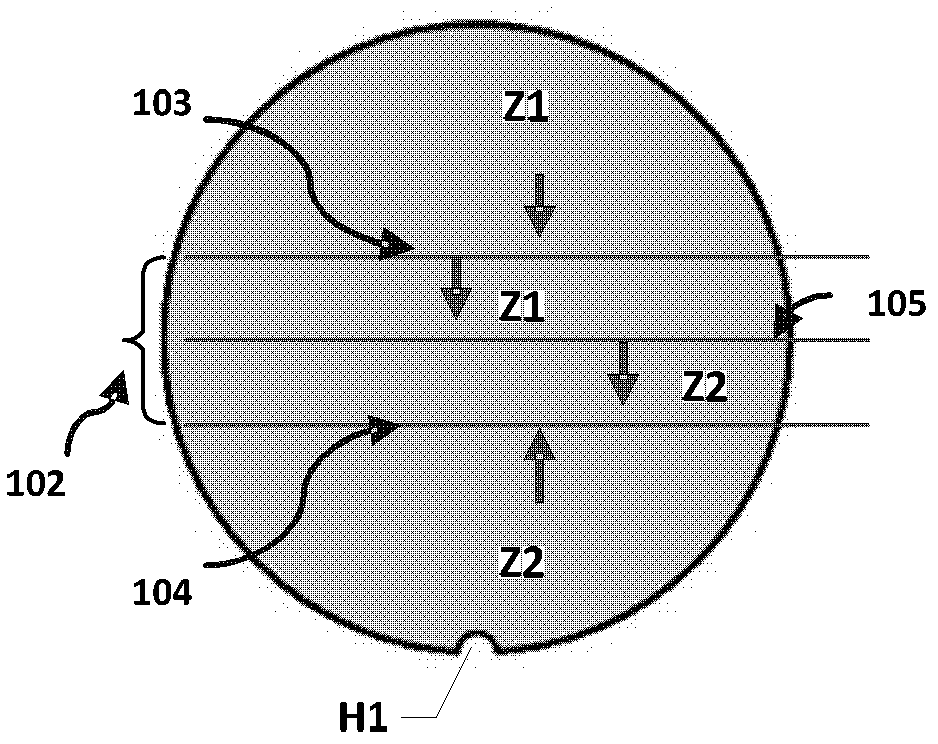
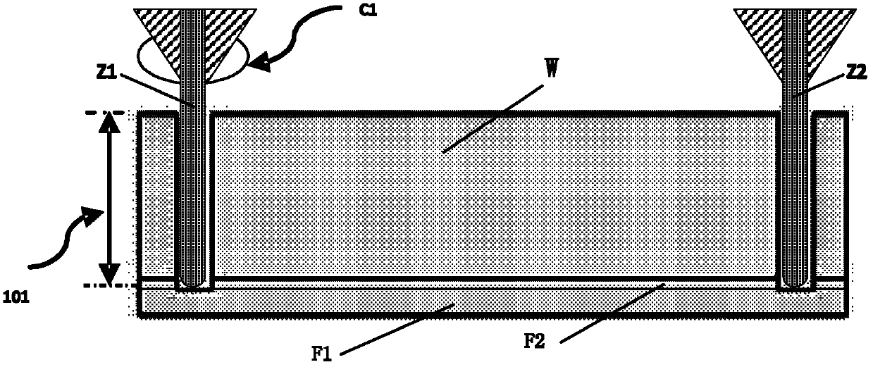
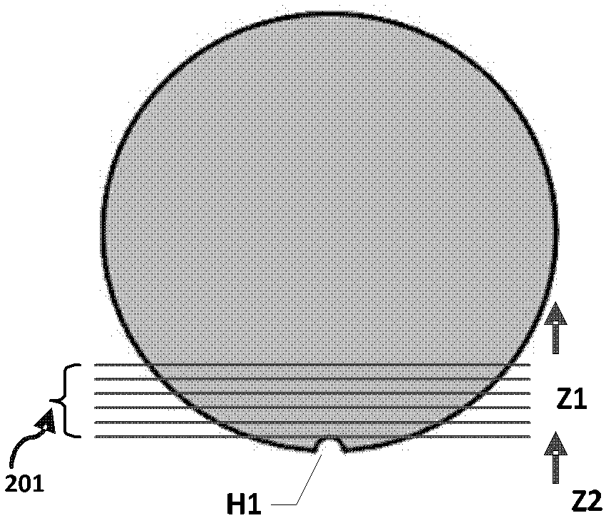
[0028] Some typical embodiments embodying the features and advantages of the present invention will be described in detail in the description in the following paragraphs. It should be understood that the invention is capable of various changes in different examples without departing from the scope of the invention, and that the descriptions and illustrations therein are illustrative in nature rather than limiting the invention.

[0029] see image 3 , image 3 It is a schematic diagram of the action of an embodiment of the method for cutting a glass wafer with two knives and two knives according to the present invention. As shown in the figure, the glass wafer W has an upper surface and a lower surface (back surface), and the back surface of the glass wafer W also has a black film F2 cured after a high-temperature film sticking process, and is pasted on the black film F2 through a patch process. Under the blue film F1. A plurality of glass wafer workpieces to be processed a...


PUM


Abstract

The invention discloses a cutting method used for chip scale package glass with a black film attached to the back face. The cutting method comprises the following steps of: fixing a first tool and a second tool on the same feed unit by taking safe distance as an interval; positioning the first tool and the second tool in an initial cutting position by the feed unit; cutting apart the surface of a chip scale package glass workpiece to form a first shear mark by the first tool in a preset feed direction, wherein the depth of the first shear mark is less than the thickness of the chip scale package glass; enabling the second tool to follow the first tool in the feed direction which is the same as that of the first tool to cut off the chip scale package glass workpiece and the black film after the feed distance of the first tool exceeds the safety distance between the first tool and the second tool on the basis of the first shear mark by a second shear mark which the is less than the first shear mark in width, and stopping in a blue film; and continuously feeding the first tool and the second tool, and repeating the cutting steps. According to the method, the edge breakage problem brought by a traditional cutting method used for the chip scale package glass is reduced, and the black film is prevented from falling off and remaining on the blue film.

Description

technical field [0001] The invention relates to a method for cutting a glass wafer (Chip Scale Package Glass, CSPG for short). Background technique [0002] With the development of wireless communication technology, high requirements are put forward for integrated circuit technology, especially the miniaturization of communication equipment makes the semiconductor chip technology develop rapidly. In the field of high frequency and radio frequency, such as wireless communication, glass wafer (CSPG) workpieces emerge as the times require, which are especially used in mobile phone components. [0003] The wafer processing process generally goes through crystal growth, cutting, outer diameter rolling, flat edge, slicing, chamfering, grinding, corrosion, polishing, cleaning, packaging and other stages. In recent years, the rapid development of photovoltaic power generation and semiconductor industry has put forward higher requirements for wafer processing: on the one hand, in or...

Claims


Application Information

Patent Timeline
Patent Type & Authority Applications(China)
IPC IPC(8): B28D5/04
Inventor 王红朱亮娟
Owner SHENZHEN STS MICROELECTRONICS CO LTD
Learn More