Laser processing apparatus

A laser processing and laser technology, which is applied in the direction of fine working devices, metal processing, stone processing equipment, etc., can solve problems such as difficult to connect cracks, difficult to cut wafers, etc., to achieve the effect of realizing production capacity and reducing the number of scans

Inactive Publication Date: 2007-03-07
OLYMPUS CORP
View PDF7 Cites 27 Cited by
  • Summary
  • Abstract
  • Description
  • Claims
  • Application Information

AI Technical Summary

Problems solved by technology

In other words, when the distance between the cracks is large, it

Method used


Image

  • Laser processing apparatus
  • Laser processing apparatus
  • Laser processing apparatus

Examples


Embodiment Construction

[0127] Hereinafter, preferred embodiments of the present invention will be described with reference to the drawings.

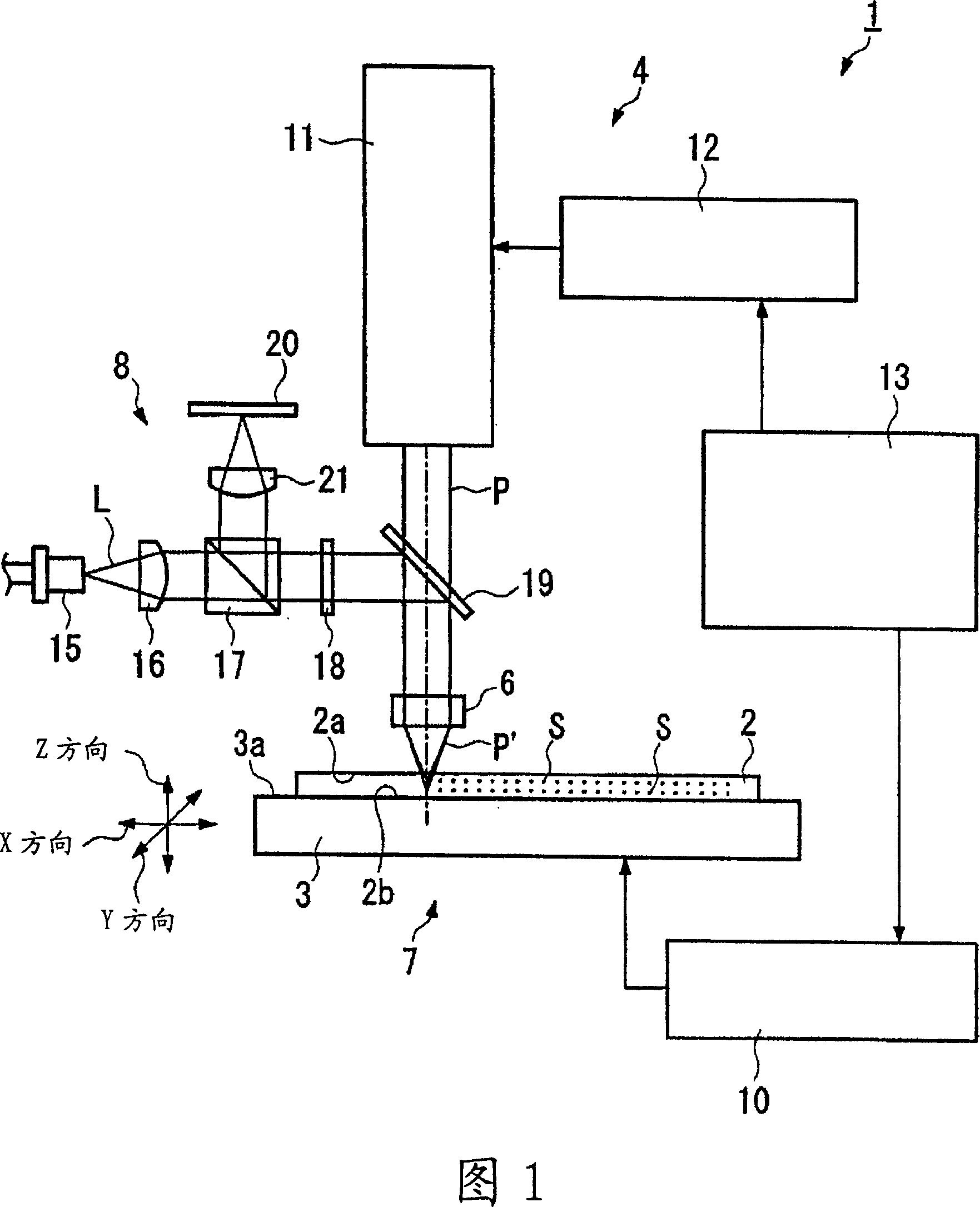
[0128] A first embodiment of the laser processing apparatus of the present invention will be described with reference to FIGS. 1 to 3 . The laser processing apparatus 1 of the present embodiment will be described as an apparatus for finely cutting a circular wafer (object to be processed) 2 having a thickness of, for example, 0.1 mm into sheets by laser processing.

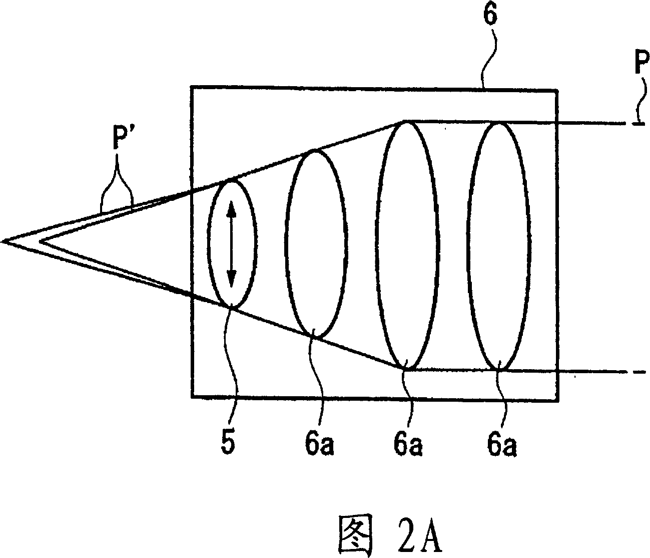
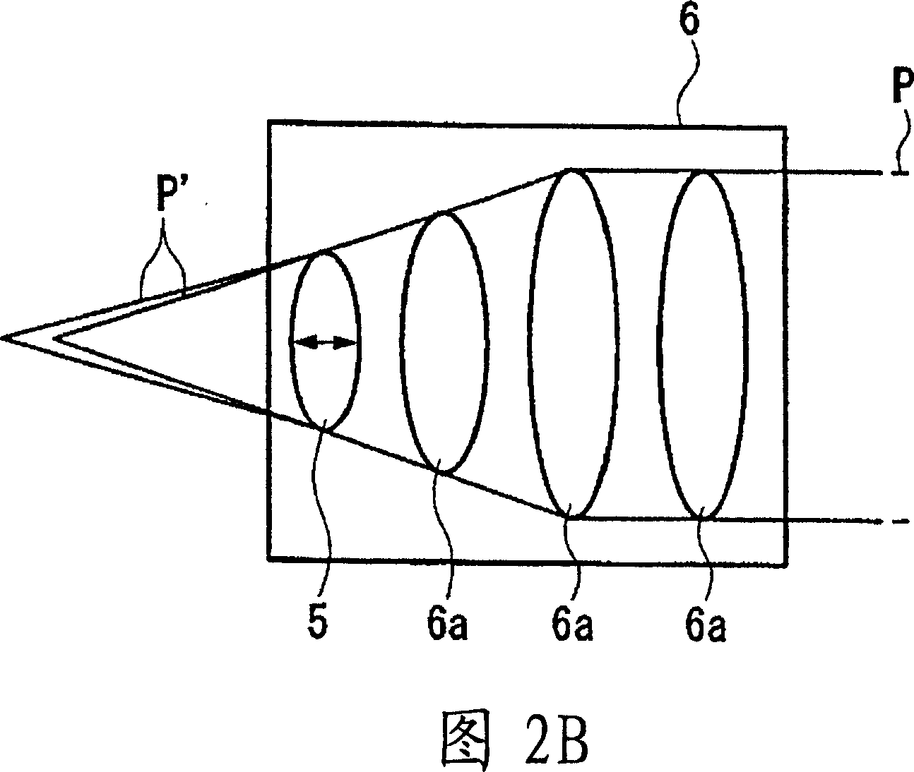
[0129] As shown in FIG. 1, the laser processing apparatus 1 includes: a table 3, which places a wafer 2 on a mounting surface 3a arranged parallel to a horizontal plane; an irradiation unit 4, which emits pulses to the surface 2a of the wafer 2. Laser (laser) P; objective lens (optical system, light-gathering optical system) 6, it has birefringent birefringent material lens (optical axis direction separation element) 5, this birefringent material lens 5 separates pulsed laser light P into multiple...


PUM


Abstract

A laser machining apparatus, provided with a stage on which a workpiece is placed, an emission device for emitting laser light toward a surface of the workpiece, an optical system for splitting the laser light into a plurality of beams, and for focusing the beams as a plurality of spots on the surface of or within the workpiece, and a movement device for moving the plurality of spots in a horizontal direction relative to the workpiece.

Description

technical field [0001] The present invention relates to laser processing equipment used for cutting semiconductor material substrates such as silicon wafers used in semiconductor devices, transparent substrates of large-diameter glass such as liquid crystal panels / plasma displays, semiconductor material substrates, piezoelectric material substrates, glass substrates, etc. . [0002] This application claims the priority of Japanese Patent Application No. 2004-062225 and Japanese Patent Application No. 2004-062226 filed on March 5, 2004, and the contents thereof are incorporated herein. Background technique [0003] Conventionally, in order to obtain semiconductor chips by cutting a semiconductor substrate such as a silicon wafer into a lattice shape (sheet shape), a method of mechanical cutting using a cutting device or the like is generally performed. In this method, scribe lines are formed in a grid pattern on the surface of the semiconductor substrate, and a blade or the ...

Claims


Application Information

Patent Timeline
IPC IPC(8): B23K26/067B28D5/00B23K26/03B23K26/08B23K26/40B28D1/22
CPCB23K26/04B23K26/03B23K26/0057B23K26/0861B28D1/221B23K26/032G02B27/283B23K26/4075B23K26/0652B23K26/0665B23K26/067B23K26/0617B23K26/043B23K2201/40B23K26/40B23K26/53B23K2101/40B23K2103/50B23K2103/56
Inventor 森田晃正高桥进
Owner OLYMPUS CORP
Why Eureka
Try Eureka