System and method for measuring coplanarity of integrated circuit (IC) pins through multistage reflection and raster imaging

A grating imaging and measurement system technology, applied in the direction of measuring devices, optical devices, instruments, etc., can solve the problems of slow detection speed, low detection accuracy, high equipment manufacturing cost, etc.

Active Publication Date: 2013-09-18
SOUTH CHINA UNIV OF TECH +1
View PDF9 Cites 18 Cited by
  • Summary
  • Abstract
  • Description
  • Claims
  • Application Information

AI Technical Summary

Problems solved by technology

[0011] The purpose of the present invention is to realize the online measurement of the coplanarity of IC chip pins, and overcome the shortcomings and shortcomings of t

Method used


Image

  • System and method for measuring coplanarity of integrated circuit (IC) pins through multistage reflection and raster imaging
  • System and method for measuring coplanarity of integrated circuit (IC) pins through multistage reflection and raster imaging
  • System and method for measuring coplanarity of integrated circuit (IC) pins through multistage reflection and raster imaging

Examples


Embodiment Construction

[0063] In order to better understand the present invention, the present invention will be further described below in conjunction with the accompanying drawings, but the embodiments of the present invention are not limited thereto.

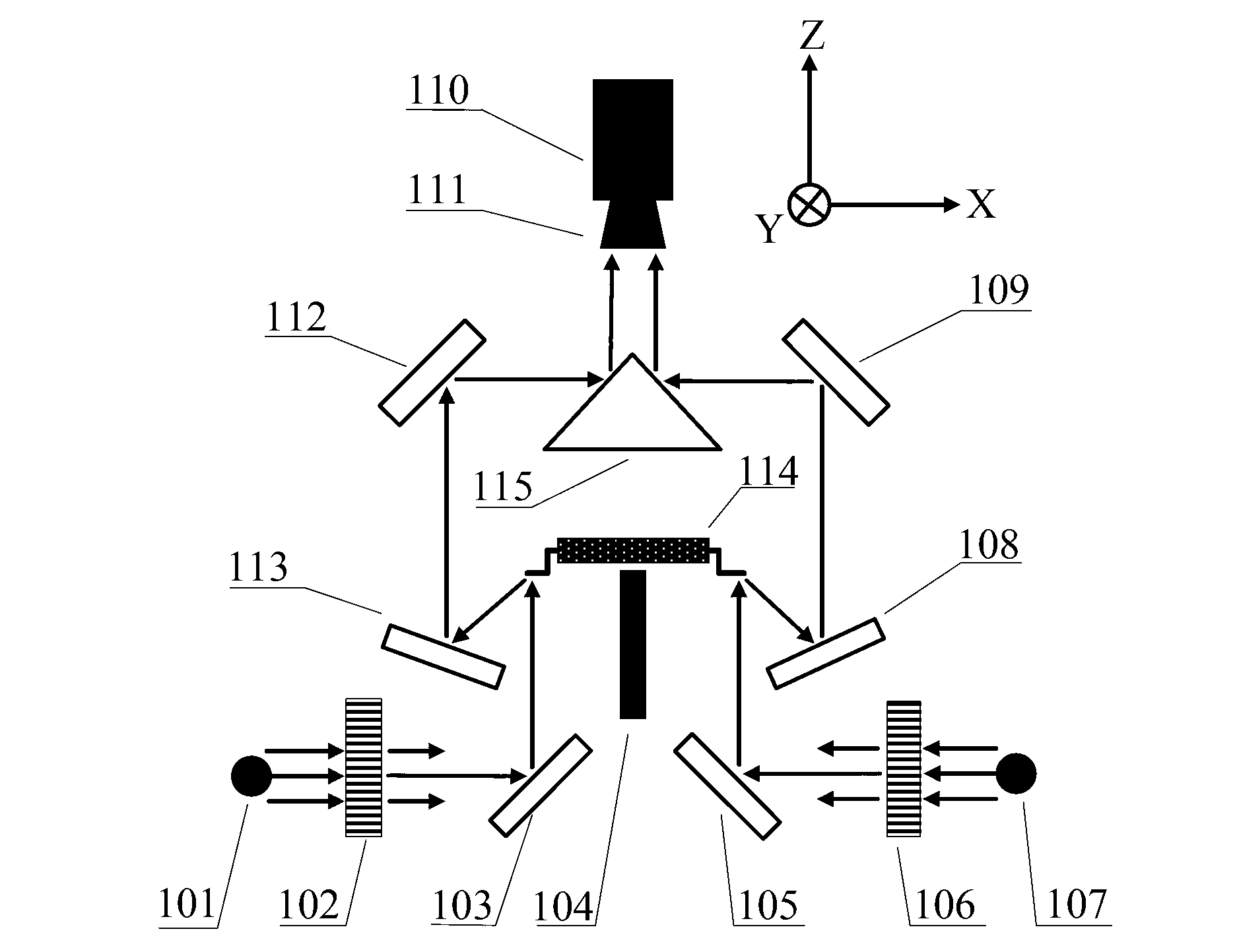
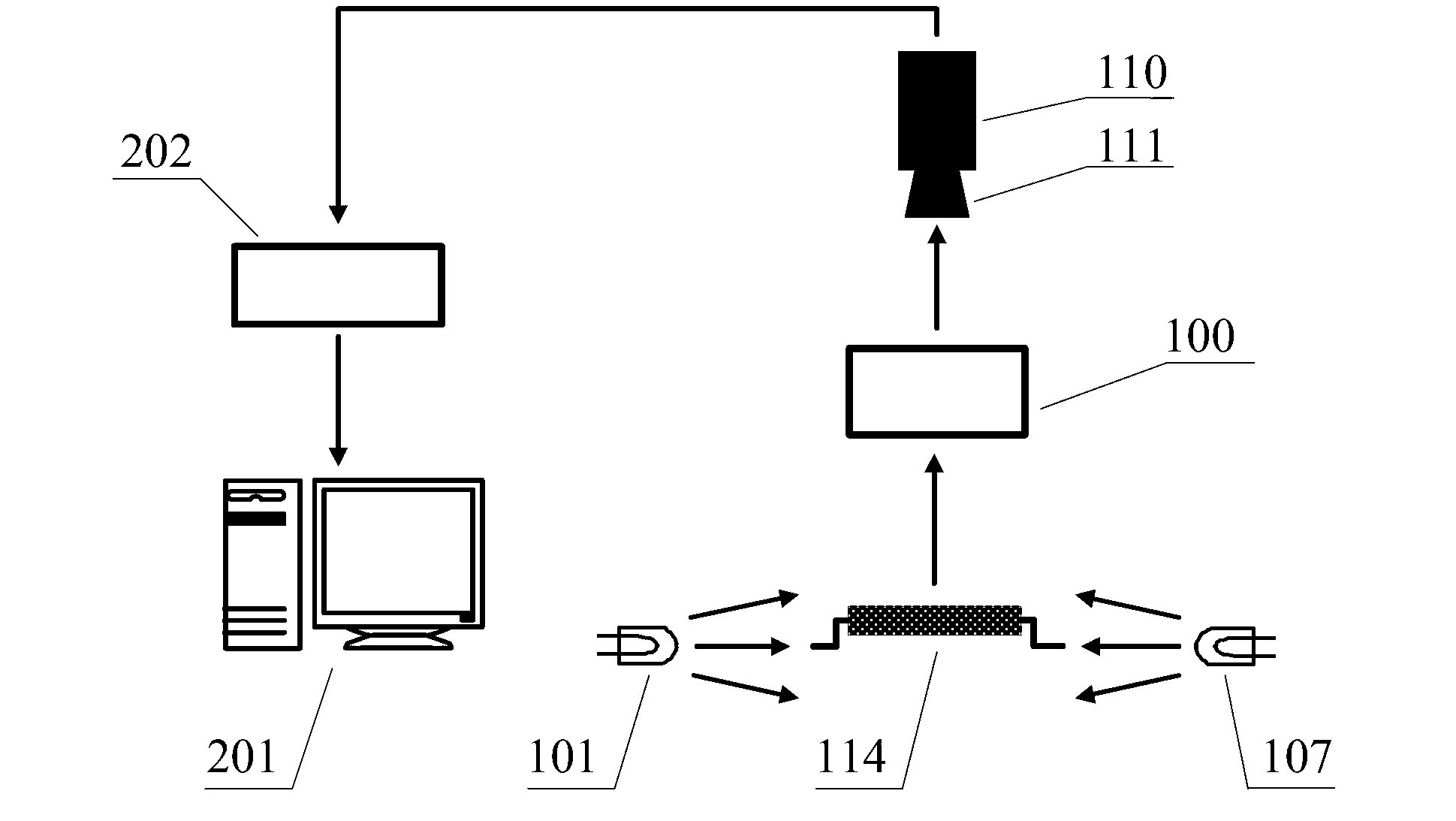
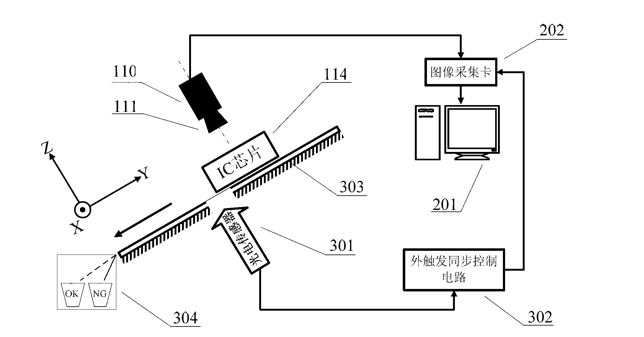
[0064] Such as figure 2 As shown, the system main frame of the present invention includes: the IC chip pin imaging optical path system 100 that multi-mirror, grating and prism constitute, IC chip self-weight oblique sliding feeding mechanism 303, image acquisition card 202, CCD camera 110 and lens 111 constitutes an imaging unit, a PC-based intelligent visual measurement system 201 , an external trigger synchronous control circuit 302 , and a superior or inferior product classification device 304 .

[0065] Such as figure 1As shown, it is the special optical path system proposed by the present invention: IC chip pin imaging optical path system 100, the left optical path of the IC chip pin imaging optical path system 100 includes: the left optical...


PUM


Abstract

The invention discloses a system and a method for measuring the coplanarity of integrated circuit (IC) pins through multistage reflection and raster imaging. The system mainly comprises an IC chip dead load slant sliding feed mechanism, an external triggering synchronous control circuit, an IC chip pin imagingoptical path system, an image acquisition card and a personal computer (PC)-based intelligent visual inspection system. The IC chip pin imaging optical path system consists of two groups of mutually independent quasi-parallel blue-light light-emitting diode (LED) light sources, two rasters, and a plurality of reflectors and prisms which areorganically combined. A raster stripe images detected from the IC chip pins can be acquired throughthe imaging optical path system; and an image acquisition and analysis software system analyzes the images of the IC chip pins with raster stripes, evaluates the isometry of the pins in the images and the torsional characteristic of the raster stripes, and calculates a corresponding coplanarity error according to a corresponding f function mapping relation between a coplanarity error and the raster stripe curved degree. By the system and the method, two rows of pins of an IC chip are simultaneously imaged, the IC chip pins can be precisely detected through one-time imaging, the structure is compact, and the cost performance is high.

Description

Technical field: [0001] The patent of the invention belongs to the field of electronic integrated circuit packaging, and specifically relates to a new method and a new system for measuring the coplanarity of IC chip pins in electronic packaging. It is suitable for real-time monitoring of pin coplanarity of large-scale integrated circuits such as DIP (Dual In-line Package, dual in-line package), SOP (Small Out-Line Package, small outline package), and PFP (Plastic Flat Package, flat package). online measurement. Background technique: [0002] With the development of surface mount technology, SMD components have achieved rapid development. In the surface mount (SMT) production process of circuit boards, in order to ensure the quality of mounting, there are certain requirements for the size and shape accuracy of the IC chip pins, especially the vertical distance from the vertex of the IC chip pins to the pad. The distance (coplanarity) has certain accuracy requirements. If t...

Claims


Application Information

Patent Timeline
IPC IPC(8): G01B11/30
Inventor 钟球盛陈忠张宪民章青春吴梓明
Owner SOUTH CHINA UNIV OF TECH
Why Eureka
Try Eureka