Method for realizing area array CMOS (complementary metal oxide semiconductor) sensor bilateral scanning clear imaging

A CMOS sensor, two-way scanning technology, used in image communication, color TV components, TV system components, etc., can solve the problems of complex hardware circuits and high costs

Inactive Publication Date: 2013-09-18
CHANGCHUN INST OF OPTICS FINE MECHANICS & PHYSICS CHINESE ACAD OF SCI
View PDF3 Cites 27 Cited by
  • Summary
  • Abstract
  • Description
  • Claims
  • Application Information

AI Technical Summary

Problems solved by technology

[0006] The present invention solves the problem that existing TDI CCD adopts the method of adding a symmetrical integral circuit when realizing bidirectional scanning imaging, which has complicated hardware circuit and high cost, and provides a method for realizing bidirectional scanning and clear imaging of an area array CMOS sensor

Method used


Image

  • Method for realizing area array CMOS (complementary metal oxide semiconductor) sensor bilateral scanning clear imaging
  • Method for realizing area array CMOS (complementary metal oxide semiconductor) sensor bilateral scanning clear imaging
  • Method for realizing area array CMOS (complementary metal oxide semiconductor) sensor bilateral scanning clear imaging

Examples


specific Embodiment approach 1

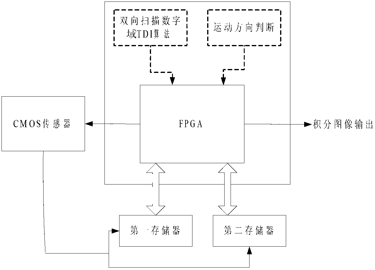
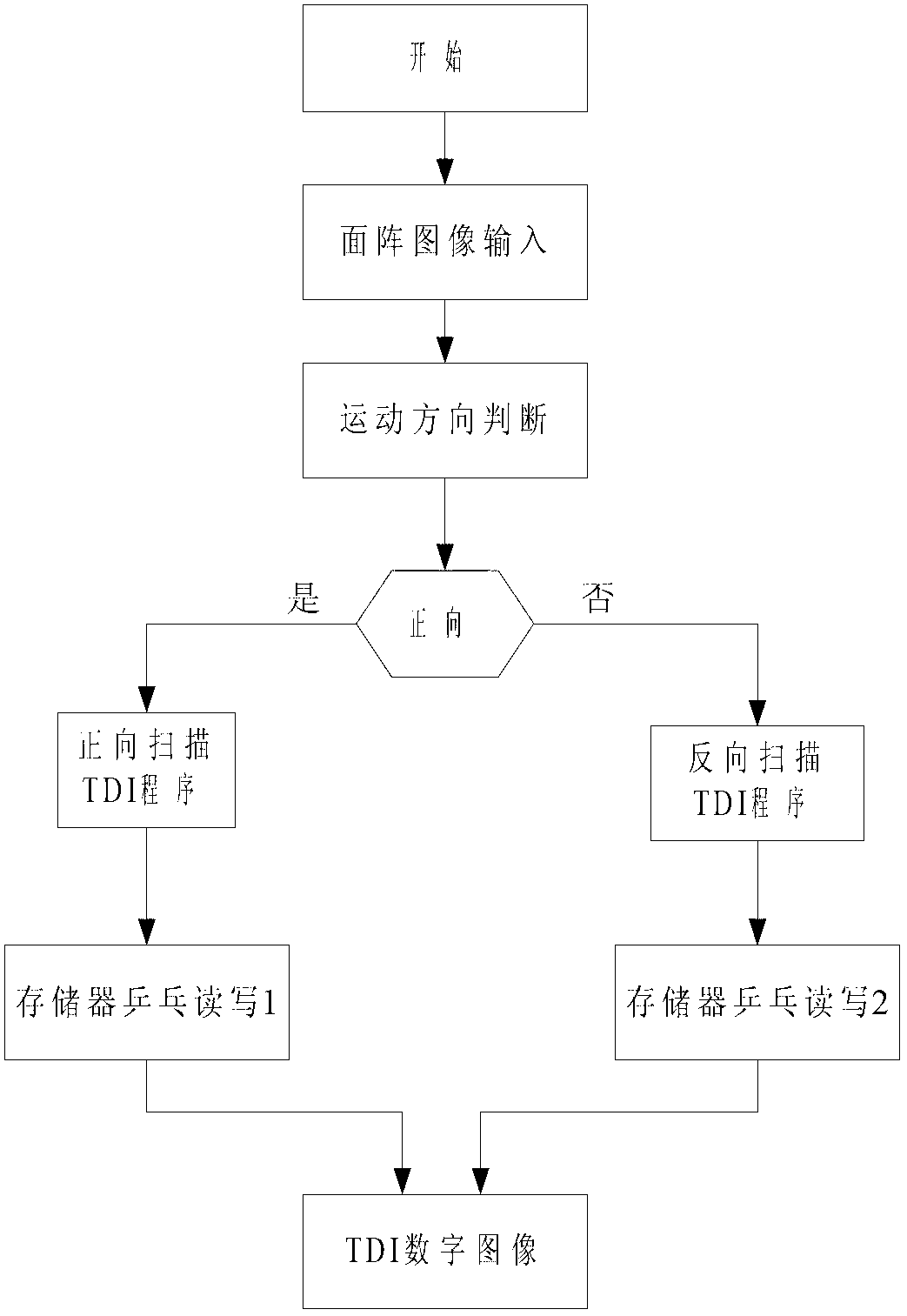
[0033] Specific implementation mode 1. Combination Figure 1 to Figure 7 Describe this embodiment, realize the method of two-way scanning and clear imaging of the area array CMOS image sensor, first acquire a frame of image by the area array CMOS sensor, then judge the current motion direction of the CMOS sensor according to the motion direction judging device, and then select the corresponding image according to the judgment result. The digital domain TDI program algorithm branch, so that the accumulation of matching image pixels can be achieved during forward and reverse scanning imaging, and a clear image can be obtained. It includes three main parts: motion direction judgment, digital domain two-way scanning TDI algorithm and memory read and write operations.

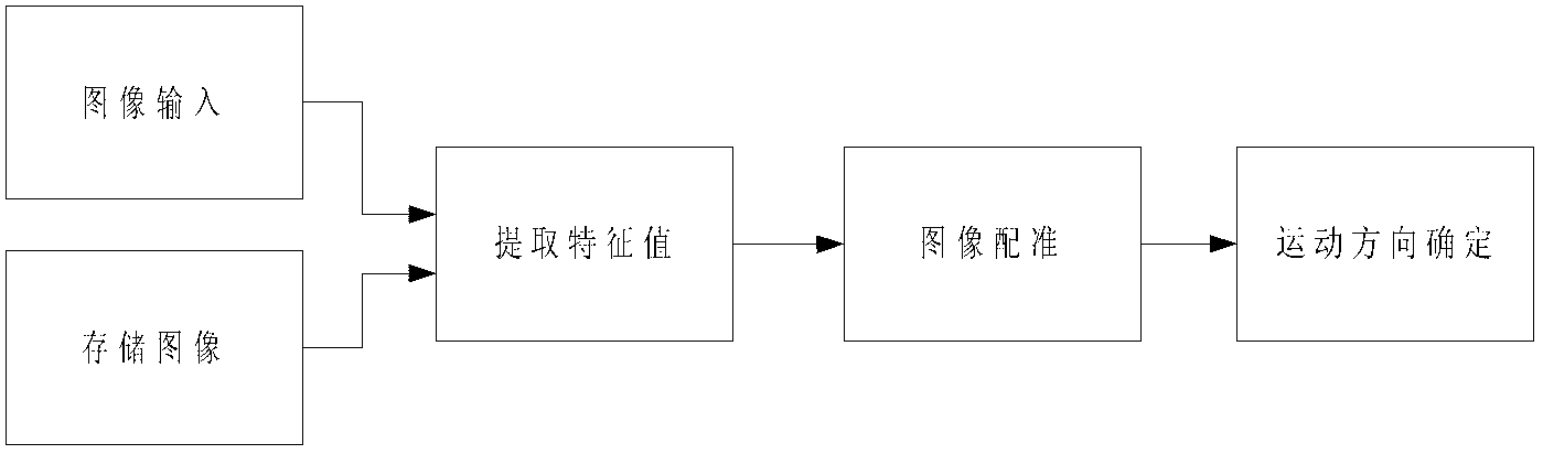
[0034] combine image 3 The motion direction judgment described in this embodiment adopts the method based on image feature matching, and according to the image processing method of extracting the feature values ​​...


PUM


Abstract

The invention discloses a method for realizing area array CMOS (complementary metal oxide semiconductor) sensor bilateral scanning clear imaging, and relates to the field of photoelectric detection imaging. The problems of complex hardware circuit and high cost due to the fact that the traditional TDICCD (time delay and integration charge coupled device) adopts a mode of increasing a symmetric integral circuit to realize bidirectional scanning imaging during bidirectional scanning imaging can be solved. The CMOS sensor is used for outputting an area array image; two off-chip memories are used for storing digital images output by the CMOS sensor; the digital image time delay integral is realized according to different TDI (time delayed and integration) control time sequences in different scanning directions; a scanning direction judgment device is used for judging the movement direction of a target scenery relative to the current sensor; according to forward scanning or reverse scanning, a targeted TDI algorithm realization mode is selected; a matched numeric field TDI algorithm can be automatically selected by numeric field bidirectional scanning TDI according to the input movement direction; and two memories are controlled to finish different read-write operations during forward scanning and reverse scanning. The method disclosed by the invention is suitable for the application of over-the-ground remote sensing.

Description

technical field [0001] The invention relates to the field of photoelectric detection and imaging, in particular to a special implementation method for bidirectional scanning and clear imaging of a CMOS image sensor. Background technique [0002] TDI (Time Delayed and Integration) technology can greatly improve the sensitivity and signal-to-noise ratio of the imaging system by accumulating multiple exposures of the same target. Space remote sensing field. Especially as people's requirements for remote sensing image resolution are getting higher and higher, TDI imaging technology is widely used in the field of high-resolution space remote sensing. [0003] At present, TDI CCDs are generally used as detectors in the field of high-resolution space remote sensing. TDI CCD is an ideal device to realize TDI, and its time delay integration process occurs in the charge domain. Driven by strict vertical transfer timing and horizontal transfer timing, charges are transferred, integr...

Claims


Application Information

Patent Timeline
IPC IPC(8): H04N5/353H04N5/374
Inventor 陶淑苹张续严金光曲宏松郑晓云贺小军
Owner CHANGCHUN INST OF OPTICS FINE MECHANICS & PHYSICS CHINESE ACAD OF SCI
Why Eureka
Try Eureka