A manufacturing method for a semiconductor device

A manufacturing method and semiconductor technology, applied in semiconductor/solid-state device manufacturing, electrical components, circuits, etc., can solve problems such as serious RC delay and large parasitic capacitance

Active Publication Date: 2013-10-02
SHANGHAI HUAHONG GRACE SEMICON MFG CORP
View PDF5 Cites 5 Cited by
  • Summary
  • Abstract
  • Description
  • Claims
  • Application Information

AI Technical Summary

Problems solved by technology

[0004] The present invention provides a manufacturing method of a semiconductor device to solve the problem of serious RC delay caused by the large parasitic capacitance between interconnection lines existing in the prior art, so as to achieve the purpose of improving the interconnection RC delay

Method used


Image

  • A manufacturing method for a semiconductor device
  • A manufacturing method for a semiconductor device
  • A manufacturing method for a semiconductor device

Examples


Embodiment Construction

[0023] The manufacturing method of the semiconductor device proposed by the present invention will be further described in detail below with reference to the accompanying drawings and specific embodiments. Advantages and features of the present invention will be apparent from the following description and claims. It should be noted that all the drawings are in a very simplified form and use imprecise scales, and are only used to facilitate and clearly assist the purpose of illustrating the embodiments of the present invention.

[0024] figure 1 The flowchart of the method for manufacturing a semiconductor device according to an embodiment of the present invention is combined below Figure 1 to Figure 8 A method of manufacturing a semiconductor device according to an embodiment of the invention will be described in detail.

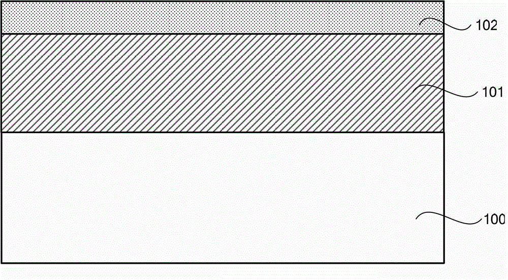
[0025] Step one, such as figure 2 As shown, a substrate 100 is provided;

[0026] The substrate 100 may be a silicon base, or a substrate on which var...


PUM


Abstract

The invention provides a manufacturing method for a semiconductor device. The manufacturing method of the invention comprises the following steps: firstly, a substrate is provided; secondly, a metal layer and a first dielectric layer are sequentially formed on the substrate through a deposition process; thirdly, the first dielectric layer and the metal layer are etched, and metal wires and first dielectric layer patterns on the metal wires are formed, and a part of the substrate is exposed; fourthly, an obstruction material layer is formed through a deposition process on the substrate and the first dielectric layer pattern; fifthly, the obstruction material layer is etched, and at least one obstruction body is formed between the adjacent metal wires; sixthly, a second dielectric layer is formed on the substrate, the first dielectric layer patterns, and the obstruction body, and gaps are formed between the metal wires and the obstruction body and / or in the second dielectric layer between the adjacent obstruction bodies. Through the adoption of the above method, the gaps can be formed in the second dielectric layer between the metal wires, and the dielectric constant of the second dielectric layer can be effectively reduced. A parasitic capacitance between the metal wires can be reduced and the condition of a RC delay of the interconnected metal wires is improved.

Description

technical field [0001] The present invention relates to a semiconductor manufacturing process, and more specifically, the present invention relates to a manufacturing method of a semiconductor device. Background technique [0002] With the continuous reduction of the feature size of semiconductor integrated circuits, the resistance capacitance delay (Resistor Capacitor, RC) of the back-end interconnection shows a significant increase trend. In order to reduce the RC delay, low dielectric constant materials are introduced, and copper interconnection replaces aluminum interconnection. become a mainstream technology. [0003] In production, with the reduction of the feature size of integrated circuits, the resistivity of copper interconnection lines will increase sharply, especially for the process of 45nm and below. However, there is currently no low-resistivity and cost-effective conductive material that can replace copper interconnects. The only way to reduce the parasitic ...

Claims


Application Information

Patent Timeline
Patent Type & Authority Applications(China)
IPC IPC(8): H01L21/768
Inventor 许丹
Owner SHANGHAI HUAHONG GRACE SEMICON MFG CORP
Why Eureka
Try Eureka