LED integration package structure based on two-sided silicon substrate and production method of structure

A technology of integrated packaging and manufacturing methods, applied in electrical components, electrical solid devices, circuits, etc., can solve the problems of large volume, complicated lamp assembly, and cost of brackets, and achieves simple lamp assembly, design flexibility, and bracket cost savings. Effect

Active Publication Date: 2013-10-02
GUANGDONG UNILUMIN ENERGY SAVINGS TECH
View PDF4 Cites 4 Cited by
  • Summary
  • Abstract
  • Description
  • Claims
  • Application Information

AI Technical Summary

Problems solved by technology

[0006] The existing LED packaging structure requires additional connection to the drive module, and requires packaging brackets, etc., which has problems such as large volume, cost of brackets, and complicated assembly of lamps.

Method used


Image

  • LED integration package structure based on two-sided silicon substrate and production method of structure

Examples


Embodiment Construction

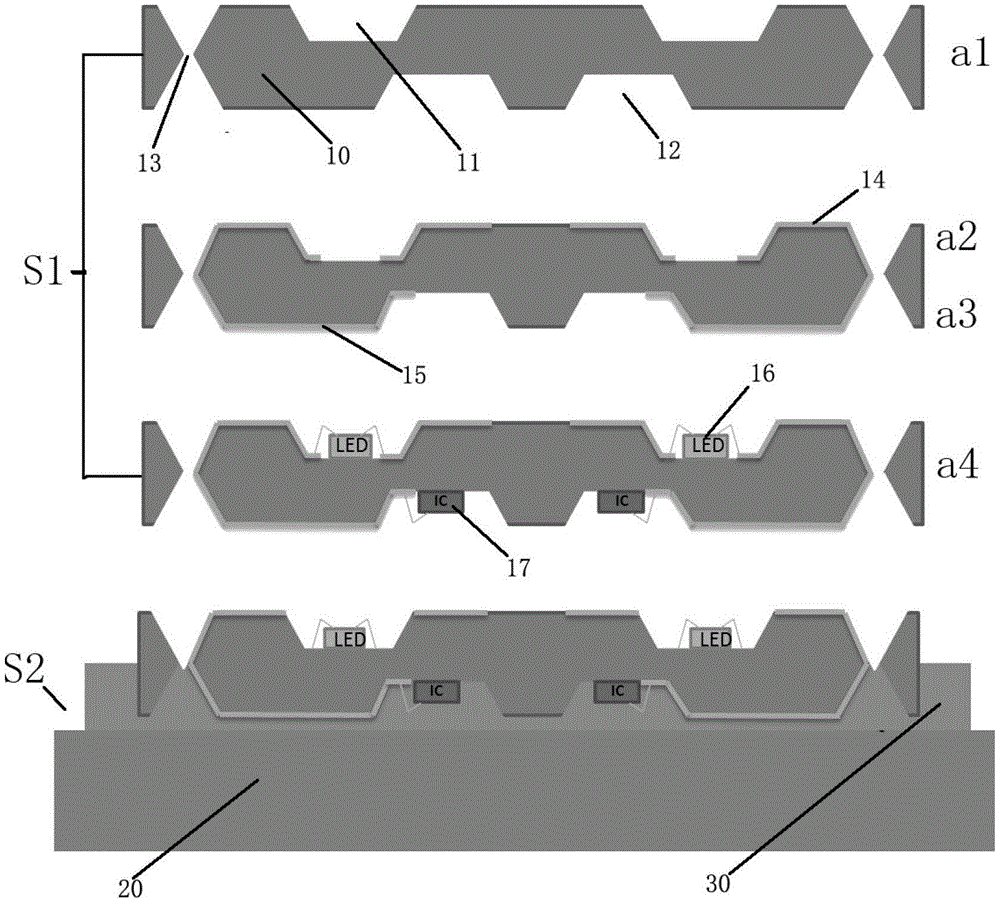
[0027] In order to describe the technical content, structural features, achieved goals and effects of the present invention in detail, the following will be described in detail in conjunction with the embodiments and accompanying drawings.

[0028] see figure 1 , an LED integrated packaging structure based on a double-sided silicon substrate in this embodiment includes an LED module and a heat sink, and the LED module is arranged on the heat sink; the LED module includes a silicon substrate 10, an LED chip 16 and a driver chip 17, one side of the silicon substrate 10 is provided with an upper layer metal wiring 14 and a first groove 11, and the LED chip 16 is packaged in the first groove 11, and the LED chip 16 is electrically connected to the upper layer metal wiring 14; the silicon substrate 10 The other side of the lower layer metal wiring 15 and the second groove 12 are provided, the driving chip 17 is packaged in the second groove 12, and the driving chip 17 is electrical...


PUM


Abstract

The invention discloses an LED (Light-emitting Diode) integration package structure based on a two-sided silicon substrate and a production method of the structure. The structure is characterized in that wires, LED chips and drive chips are integrated on the two side faces of the silicon substrate; the structure is small in size, and flexible, saves bracket cost, and does not require external drive; a lamp is simple to assemble; the wires are integrated on the silicon substrate; connections and lengths of conductors are reduced; and heat resistance of mechanical connection is reduced, so that the power loss of electric connection is lowered, and power is increased. The production method of the structure can adopt a micromachining technology; etching and wiring of a micro dimension is controlled accurately; the LED chips and the drive chips are mounted and packaged precisely; the size of the structure is decreased as far as possible; a three-dimensional package technology is adopted to integrally package elements on the two sides of the silicon substrate; the area of the substrate can be utilized sufficiently; the dimension of an LED module is decreased; an additional drive module is not required due to miniaturization of the LED module; a larger space can be made for placing other control modules due to heat sink of the lamp; and intelligent illumination is realized.

Description

technical field [0001] The invention relates to the field of LED lighting, in particular to an LED integrated packaging structure and a manufacturing method based on a double-sided silicon substrate. Background technique [0002] At present, LED packaging technology mainly includes the connection of three parts: LED module, heat sink and circuit. [0003] 1. LED module: The LED module is to package one or more LED light sources on the substrate. The most common packaging method is to package the LED chip in a bracket, and then solder the package body to the lead frame on the substrate. There are also further integrated packaging of LEDs on the substrate, and other circuits or control components, such as Zener diodes, optical sensing elements for light output and junction temperature testing, etc. are packaged on the same substrate, and the circuits on the PCB board are mutually connect. [0004] 2. Radiator: LED modules are usually connected to a radiator, and the heat ge...

Claims


Application Information

Patent Timeline
Patent Type & Authority Applications(China)
IPC IPC(8): H01L25/16H01L33/48H01L33/54
CPCH01L2224/48227
Inventor 林洺锋韦嘉徐振雷梁润园法比奥·圣阿加塔亨德里克斯·威廉默斯·范·蔡吉张春旺包厚华
Owner GUANGDONG UNILUMIN ENERGY SAVINGS TECH
Why Eureka
Try Eureka