Array substrate and liquid crystal display
An array substrate and substrate technology, applied in static indicators, instruments, nonlinear optics, etc., can solve the problems of pixel aperture ratio, bad pixel area, low resolution of TFT-LCD, etc., so as to reduce delay and improve aperture. rate, the effect of increasing the resolution
- Summary
- Abstract
- Description
- Claims
- Application Information
AI Technical Summary
Problems solved by technology
Method used
Image

Examples
Embodiment Construction
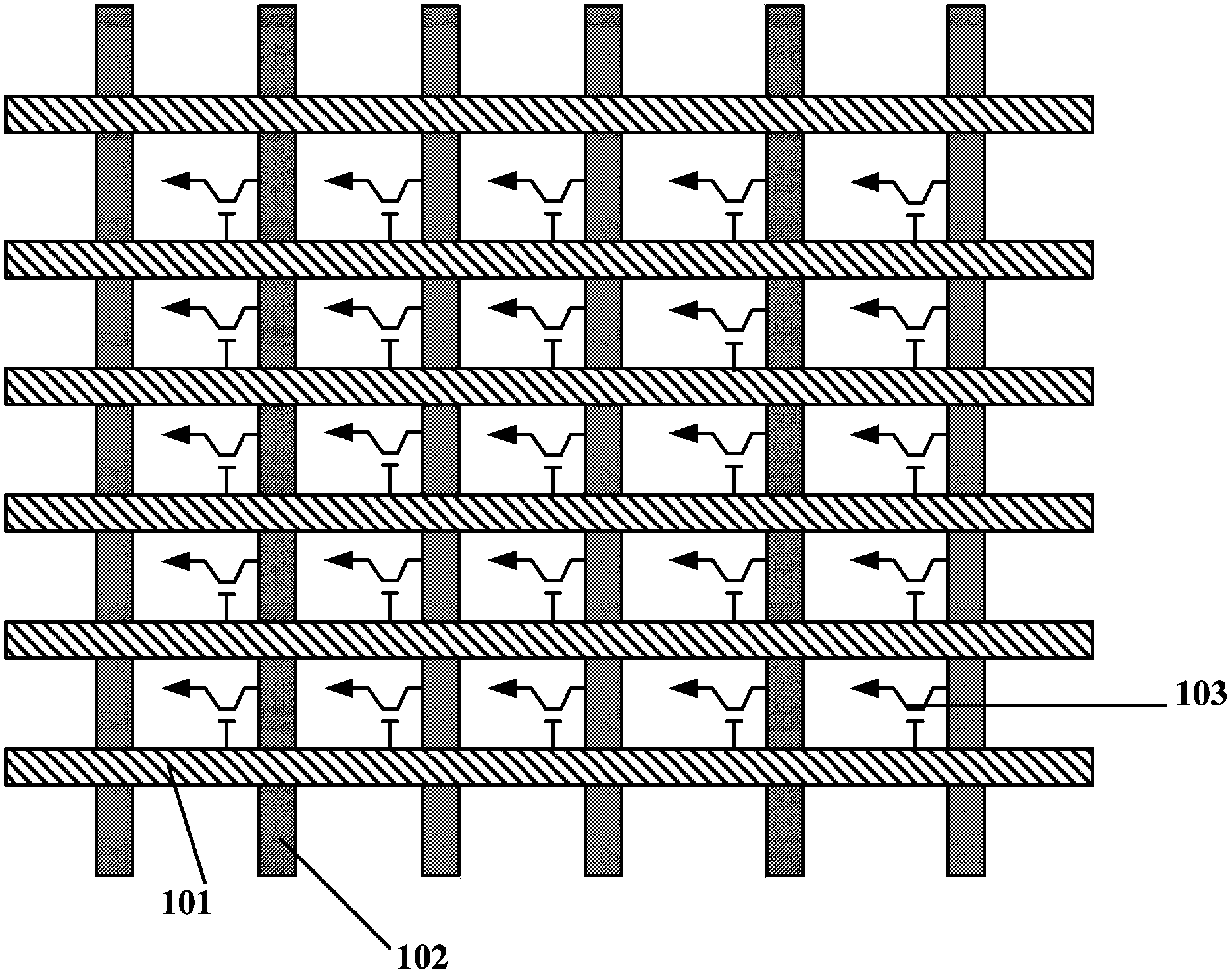
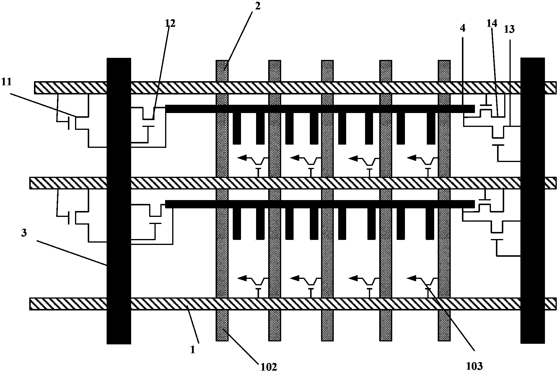
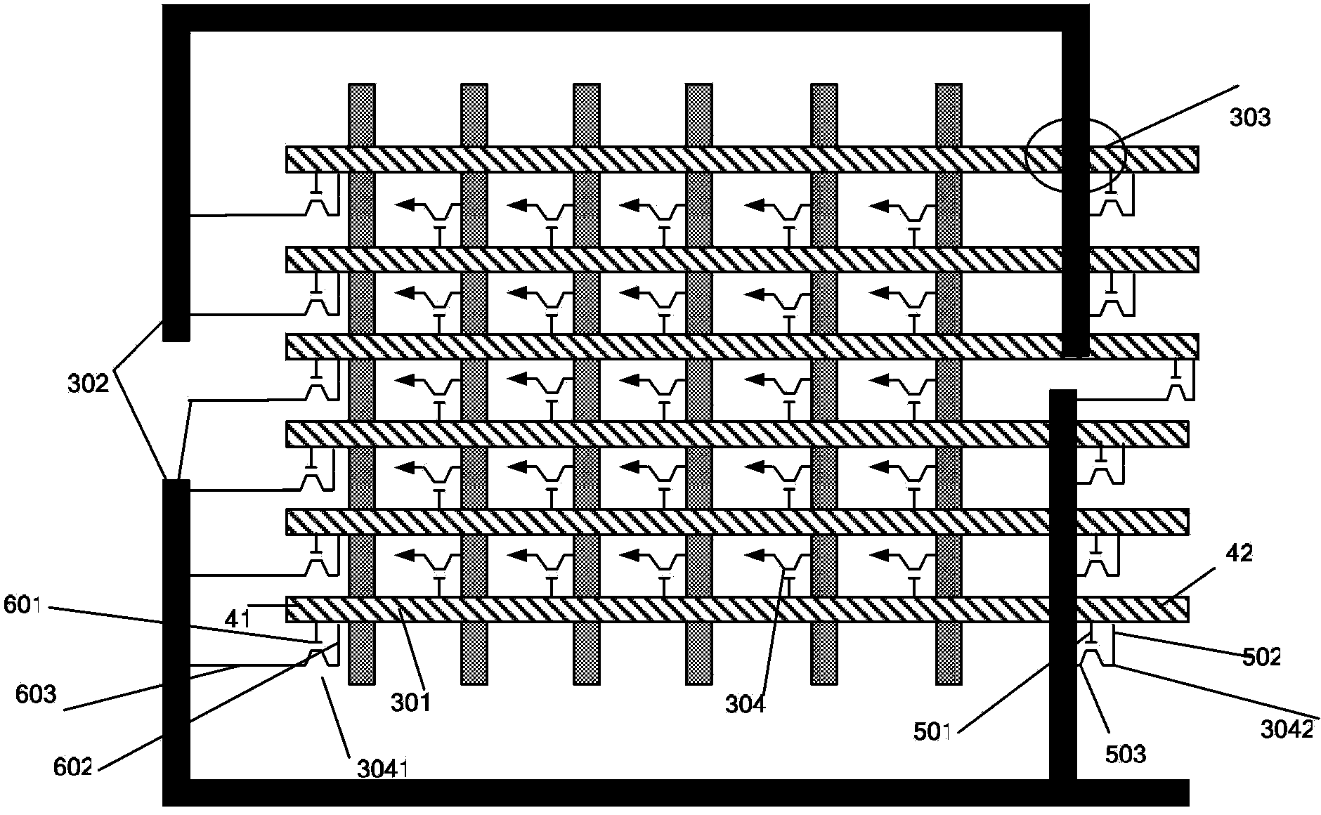
[0014] In the prior art, the gate signal of each row is simultaneously transmitted by the gate line of the row and the pixel common electrode of the next row, the number of common electrodes required is relatively large, and the common electrodes are arranged inside the pixel area, so there will be no The bad effect of the pixel area causes the aperture ratio of the pixel to be greatly limited, which in turn makes the resolution of the TFT-LCD lower. Different thin film transistors connect the two ends of the gate signal line to the provided lead wires. For each row of gate signal lines formed on the array substrate, the gate signal can pass through the row of gate signal lines and connect with the row of gate signals. The leads connected to the signal lines are conducted at the same time, and the gate signal of each row is conducted at least by the gate signal line and the set lead at the same time, which reduces the gate resistance, improves the conduction speed of the gate s...
PUM
 Abstract
Description
Claims
Application Information
 - R&D
- Intellectual Property
- Life Sciences
- Materials
- Tech Scout
- Unparalleled Data Quality
- Higher Quality Content
- 60% Fewer Hallucinations
Browse by: Latest US Patents, China's latest patents, Technical Efficacy Thesaurus, Application Domain, Technology Topic, Popular Technical Reports.
© 2025 PatSnap. All rights reserved.Legal|Privacy policy|Modern Slavery Act Transparency Statement|Sitemap|About US| Contact US: help@patsnap.com