Backside off-axis alignment system, photolithography device and method based on array photoelectric sensor

A photoelectric sensor and alignment system technology, applied in the field of integrated circuit equipment manufacturing, to achieve the effects of reducing alignment errors, easy detection, and reducing the range of motion

Active Publication Date: 2016-01-20
SHANGHAI MICRO ELECTRONICS EQUIP (GRP) CO LTD +1
View PDF4 Cites 0 Cited by
  • Summary
  • Abstract
  • Description
  • Claims
  • Application Information

AI Technical Summary

Problems solved by technology

[0008] In order to overcome the defects in the prior art, the present invention provides a backside off-axis alignment system, photolithography device and method based on an array photoelectric sensor, which can effectively avoid the problem of low alignment efficiency caused by slow response speed of CCD sensors

Method used


Image

  • Backside off-axis alignment system, photolithography device and method based on array photoelectric sensor
  • Backside off-axis alignment system, photolithography device and method based on array photoelectric sensor
  • Backside off-axis alignment system, photolithography device and method based on array photoelectric sensor

Examples


Embodiment Construction

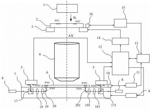
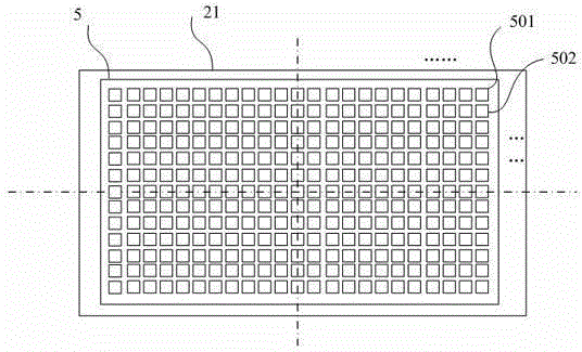
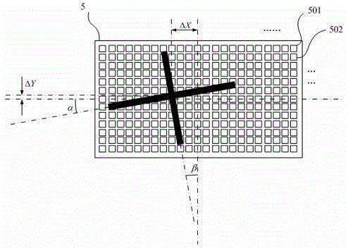
[0025] The back off-axis alignment system, lithography apparatus and method of a specific embodiment of the present invention will be described in detail below with reference to the accompanying drawings. However, it should be understood that the present invention is not limited to the embodiment described below, and the technical idea of ​​the present invention can be implemented in combination with other known technologies or other technologies having the same functions as those known technologies.

[0026] In the following description, in order to clearly show the structure and working mode of the present invention, many directional words will be used for description, but the words "front", "rear", "left", "right", "outer", "inner" should be used. "", "outward", "inward", "上", "下" and other words are understood as convenient terms and should not be understood as restrictive terms. In addition, the term "X-direction" used in the following description mainly refers to the horizo...


PUM


Abstract

The invention discloses a backside off-axis alignment system based on an array photoelectric sensor, which is used to determine the relative positional relationship between a substrate and a workpiece table, wherein the workpiece table has a first surface and a second surface opposite to the second surface. a surface for supporting the substrate and providing movement of the substrate, the back of the substrate is in contact with the first surface of the workpiece table, and the alignment system includes: an imaging optical system for at least one alignment mark on the back of the substrate An image is formed above the first surface of the workpiece table; an array photoelectric sensor is used to detect the image of the alignment mark, wherein the array sensor includes a plurality of photoelectric sensors separated from each other, and the size of the photosensitive surface of each photoelectric sensor is larger than the alignment mark The distance between the photosensitive surfaces of any two photosensors is smaller than the minimum size of the image of the alignment mark; the control module is used to collect and process the image information of the alignment mark to determine the position of the back side of the substrate The position information of the alignment mark.

Description

technical field [0001] The invention relates to the field of integrated circuit equipment manufacturing, in particular to a backside off-axis alignment system based on an array photoelectric sensor, a photolithography device and a method. Background technique [0002] With the continuous improvement of people's living standards and the development of semiconductor technology, the semiconductor market will continue to increase the requirements for the intelligence and miniaturization of semiconductor packaging devices in the future. Digital products such as cameras, mobile phones, and PDAs are not only required to be small and easy to carry. It is also required to have multiple functions and low cost performance. In order to achieve the development requirements of intelligent and miniaturized packaging devices, there is a need for multi-silicon chip packaging solutions. Multi-wafer packaging is a silicon wafer-level packaging method that stacks and connects two or more plana...

Claims


Application Information

Patent Timeline
Patent Type & Authority Patents(China)
IPC IPC(8): G03F7/20G03F9/00
Inventor 唐文力王海江
Owner SHANGHAI MICRO ELECTRONICS EQUIP (GRP) CO LTD
Why Eureka
Try Eureka