Chip welding device and method using same

A chip welding and chip technology, which is applied in welding equipment, water conservancy projects, marine engineering and other directions, can solve the problem of high cost of device manufacturing and other problems

Active Publication Date: 2006-09-20
SAMSUNG ELECTRONICS CO LTD
View PDF0 Cites 10 Cited by
  • Summary
  • Abstract
  • Description
  • Claims
  • Application Information

AI Technical Summary

Problems solved by technology

[0009] However, if the chip bonding device with two wafer logistics is designed as the structure of the existing chip bonding device, then in order to ensure the plane range of movement of the two wafer mounts and the range of move

Method used


Image

  • Chip welding device and method using same
  • Chip welding device and method using same
  • Chip welding device and method using same

Examples


Embodiment Construction

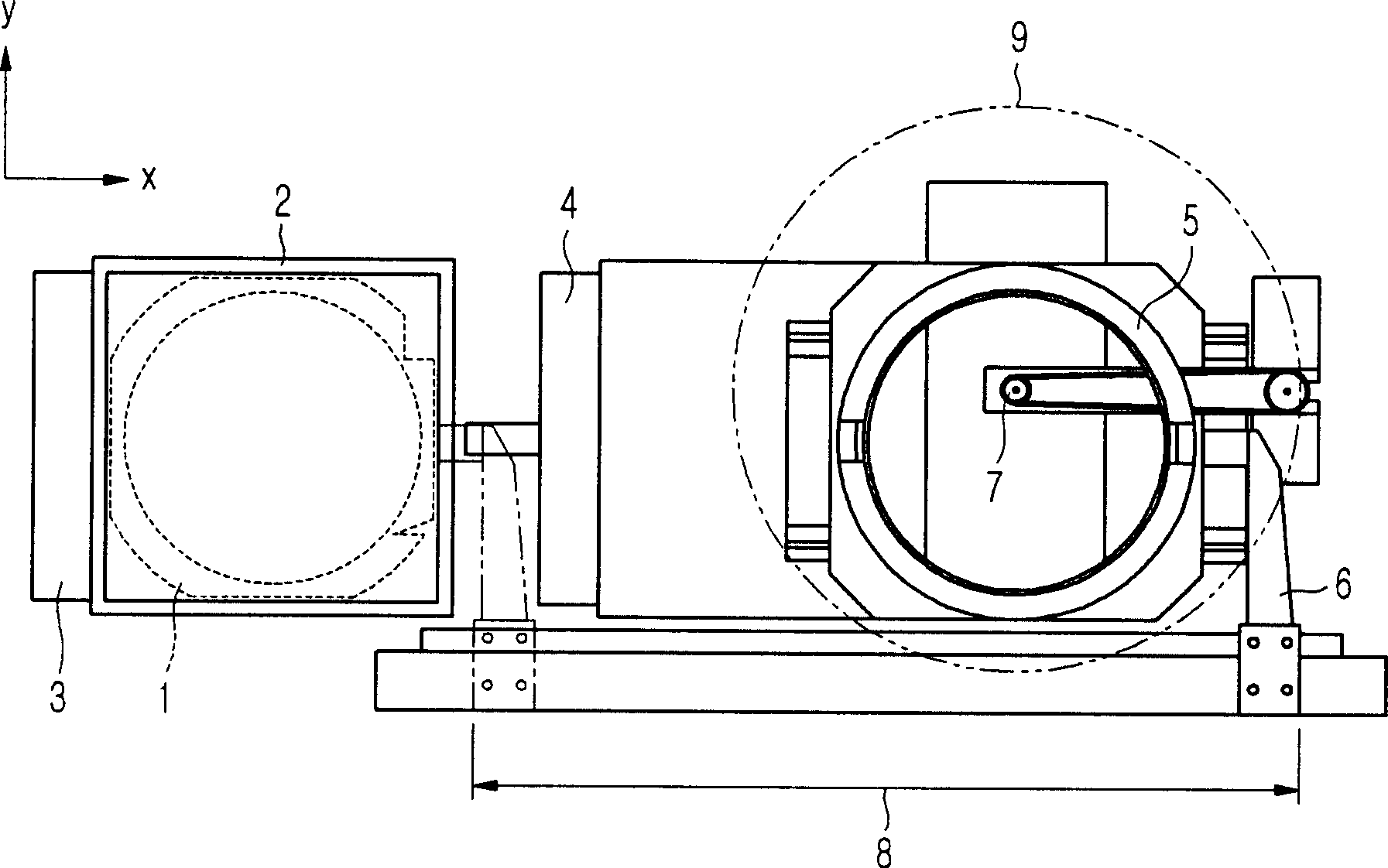
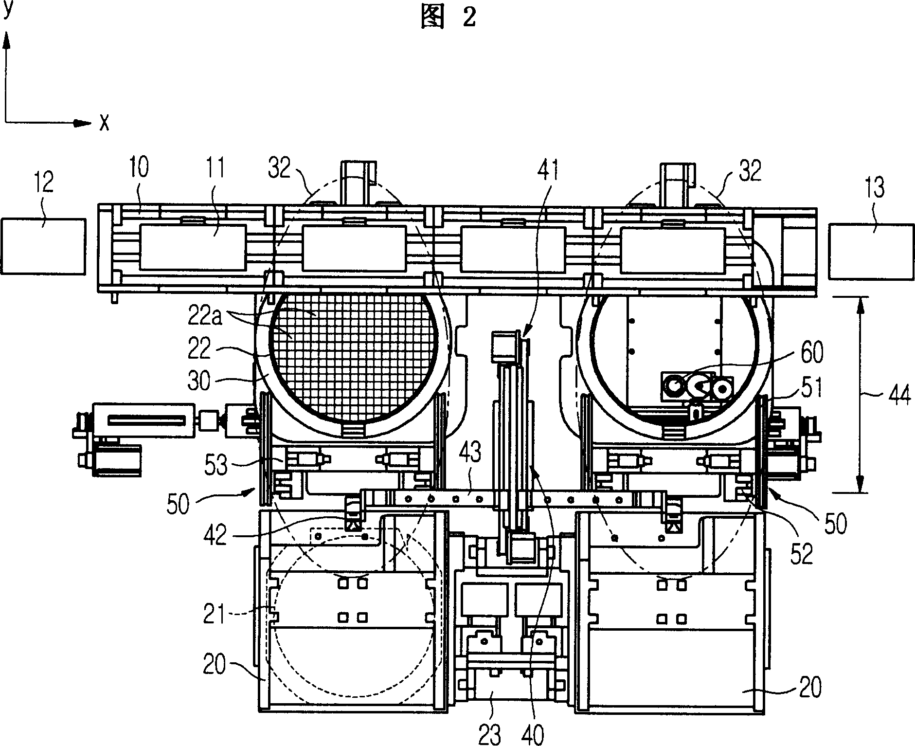
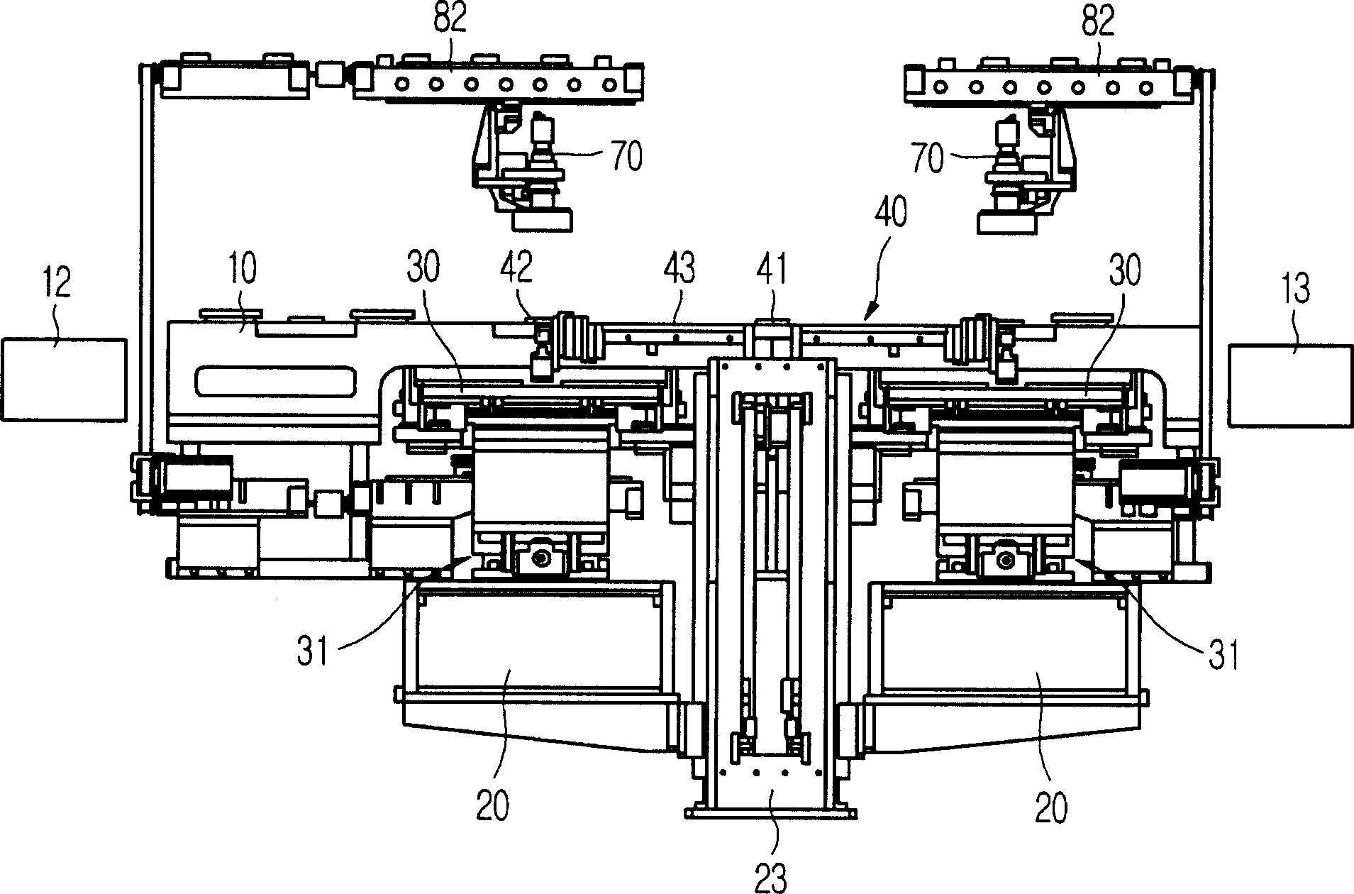
[0027] Hereinafter, embodiments according to the present invention will be described in detail with reference to the accompanying drawings. Fig. 2 is a schematic plan view showing a chip bonding device provided according to the present invention, image 3 It is a schematic front view showing a chip bonding device provided according to the present invention.

[0028] Figure 2 and image 3 As shown, the die bonding apparatus provided according to the present invention includes a lead frame moving part related to lead frame movement, a wafer moving part related to wafer loading and unloading and wafer movement for determining the position of a chip to be picked up, and a wafer moving part related to wafer movement. The chip moving part related to Die Attach that picks up the chip and attaches it to the lead frame.

[0029] The lead frame moving part is located on the rear side of the device, and includes an indicator track 10 for carrying and transferring the lead frame 11, and...


PUM


Abstract

The invention discloses a chip welding device which can shorten the chip motion range and improve the chip transfer method to reduce the device volume when picking up the chip and relative chip welding method. Wherein, the chip support makes single-axle motion different from the plane motion, to reduce the motion range of chip support to one axle; and using one driving unit to drive the extrusion device and the chip camera to move vertical to the motion of chip support; and it arranges a rotation device between the chip box and the chip support when loading the chip to reduce the motion range of moving element. The invention can attain economic benefits, while one device can effectively weld several chips.

Description

technical field [0001] The present invention relates to a device for semiconductor packaging process, in particular to a chip bonding device which reduces the size of the device by shortening the movement range of the chip when picking up the chip and improving the method of transferring the chip when loading and unloading the chip, and a chip using the device Welding method. Background technique [0002] Usually, the semiconductor packaging manufacturing process includes the cutting (Sawing) process of cutting the wafer into a single semiconductor chip, the die bonding (Die Bonding) process of attaching a single semiconductor chip to the lead frame (Lead Frame), and the electrical connection of the semiconductor chip and the lead frame wire. Wire bonding (Wire Bonding) process, molding (Molding) process of wrapping around the semiconductor chip to protect the internal circuit and other parts of the semiconductor chip, trimming (Trim) / forming (Form)...

Claims


Application Information

Patent Timeline
IPC IPC(8): H01L21/60H01L21/50B23K31/00
CPCE02B7/44E02B7/46E05Y2201/454E05Y2201/456E05Y2600/322E05Y2900/40
Inventor 石承大金秋浩李炳俊
Owner SAMSUNG ELECTRONICS CO LTD
Why Eureka
Try Eureka