Light emitting apparatus and its driving method

A light-emitting device and light-emitting element technology, which is applied to lighting devices, electroluminescent light sources, light sources, etc., can solve the problem of difficulty in miniaturizing light-emitting devices, and achieve the effect of miniaturization and high contrast.

Inactive Publication Date: 2013-10-23
CANON KK
View PDF4 Cites 4 Cited by
  • Summary
  • Abstract
  • Description
  • Claims
  • Application Information

AI Technical Summary

Problems solved by technology

[0004] However, according to Japanese Patent Application Laid-Open No. 2010-262251, since a transistor for connecting a dedicated reference voltage line and a drive circuit and control wiring for such a transistor are required in order to extract unnecessary charges, the number of constituent parts increases. As a result, it is difficult to realize the miniaturization of light-emitting devices
Therefore, the technique disclosed in Japanese Patent Application Laid-Open No. 2010-262251 is not suitable for the case where miniaturization of the light emitting device is required

Method used


Image

  • Light emitting apparatus and its driving method
  • Light emitting apparatus and its driving method
  • Light emitting apparatus and its driving method

Examples


Embodiment 1)

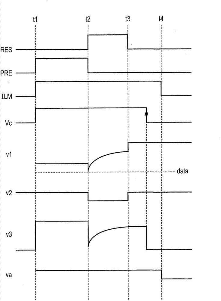
[0064] In this example, according to Figure 5 The timing diagram, by using Figure 4 The drive circuit in to drive the device.

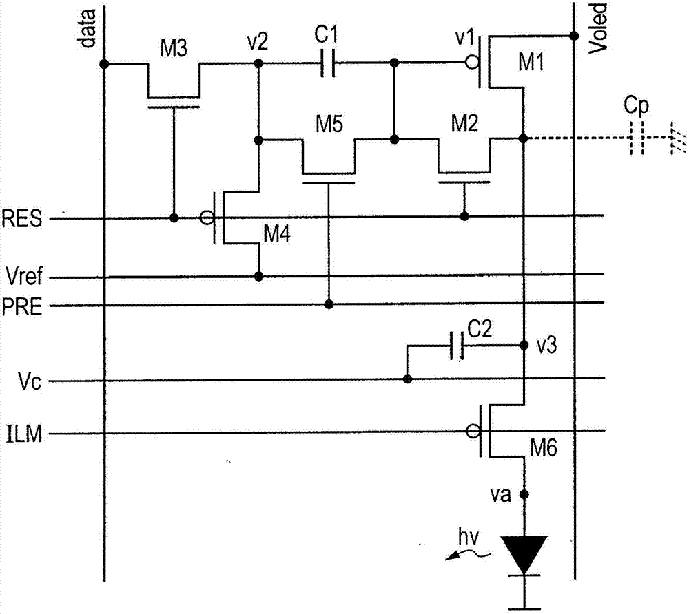
[0065] Figure 4 The drive circuit in the figure 1 The difference of the driving circuit in is that the scanning signal ILM is supplied instead of the control signal Vc. Since there is no need to provide wiring for a control signal line for supplying the control signal Vc, it is expected that the size of the light emitting element can be reduced.

[0066] At time t4, the scanning signal ILM changes from H to L. In order to set the drain voltage (v3) of the driving transistor to a value equal to or lower than the threshold voltage for initiating light emission of the EL, when it is assumed that the amplitude of the scanning signal ILM is equal to ΔVilm, the capacitance value of the capacitor C2 is set to satisfy the following The value of the condition.

[0067] C2≥Cp / [{ΔVilm / (Voled–Vth-ELVth)}–1]

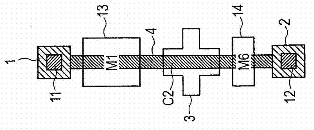
[0068] exist Figures 6A-6C A method of for...

Embodiment 2)

[0078] In this example, according to Figure 9 The timing diagram, by using Figure 8 The drive circuit in to drive the device.

[0079] Figure 8 The drive circuit in the figure 1 The difference of the drive circuit in 2 is that the scan signal RES is supplied instead of the control signal Vc. Since there is no need to provide wiring for a control signal line for supplying the control signal Vc, it is expected that the size of the light emitting element can be reduced.

[0080] At time t3, the scanning signal RES changes from H to L. In order to set the drain voltage (v3) of the drive transistor to a value equal to or lower than the threshold voltage for initiating light emission of the EL, when it is assumed that the amplitude of the scan signal RES is equal to ΔVres, the capacitance value of the capacitor C2 is set to satisfy the following The value of the condition.

[0081] C2≥Cp / [{ΔVres / (Voled–Vth-ELVth)}–1]

[0082] As a method of forming the capacitor C2 in this...


PUM


Abstract

A light emitting apparatus wherein, after setting a voltage of a light emitting luminance into a gate of the driving transistor, until setting a light emission controlling transistor at an electrically conducting state, a control signal changing toward a voltage of an opposite electrode of the light emitting element is supplied to the other terminal of the capacitor constructed such that an electro-conductive layer supplied with the control signal and a semiconductor layer forming the terminal of the driving transistor at the side of the light emitting element, a semiconductor layer forming a terminal of a transistor different from the driving transistor and connected to the terminal of the driving transistor at the side of the light emitting element, or an electro-conductive layer connected to the terminal of the driving transistor at the side of the light emitting element are formed so as to face through an insulating layer.

Description

technical field [0001] The present invention relates to a light emitting device having a light emitting element and a driving method of the light emitting device, and more particularly, to a light emitting device and a driving method of the light emitting device for controlling light emission of an organic electroluminescence (EL) element as a current control element. Background technique [0002] As a drive circuit for driving an organic EL (hereinafter, simply referred to as "EL"), there is a drive circuit having a configuration in which a data voltage according to gradation data is supplied to the gate of a drive transistor and A current is supplied to the EL connected to the source or drain of the drive transistor. According to a light-emitting device using EL as a light-emitting element of such a drive circuit, black luminance can be set to zero and infinite contrast can be realized in principle. However, when the source or drain of the driving transistor has a parasit...

Claims


Application Information

Patent Timeline
Patent Type & Authority Applications(China)
IPC IPC(8): G09G3/32H05B44/00
CPCH05B33/08H05B33/0824H05B45/44H05B45/00Y02B20/30H05B44/00
Inventor 池田宏治
Owner CANON KK
Why Eureka
Try Eureka