Non-volatile memory device and method of operating the same
A non-volatile storage and device technology, applied in the field of semiconductor circuits, can solve the problems that PRAM does not support different storage units to set data and reset data, errors, read data damage, etc.
- Summary
- Abstract
- Description
- Claims
- Application Information
AI Technical Summary
Problems solved by technology
Method used
Image

Examples
Embodiment Construction
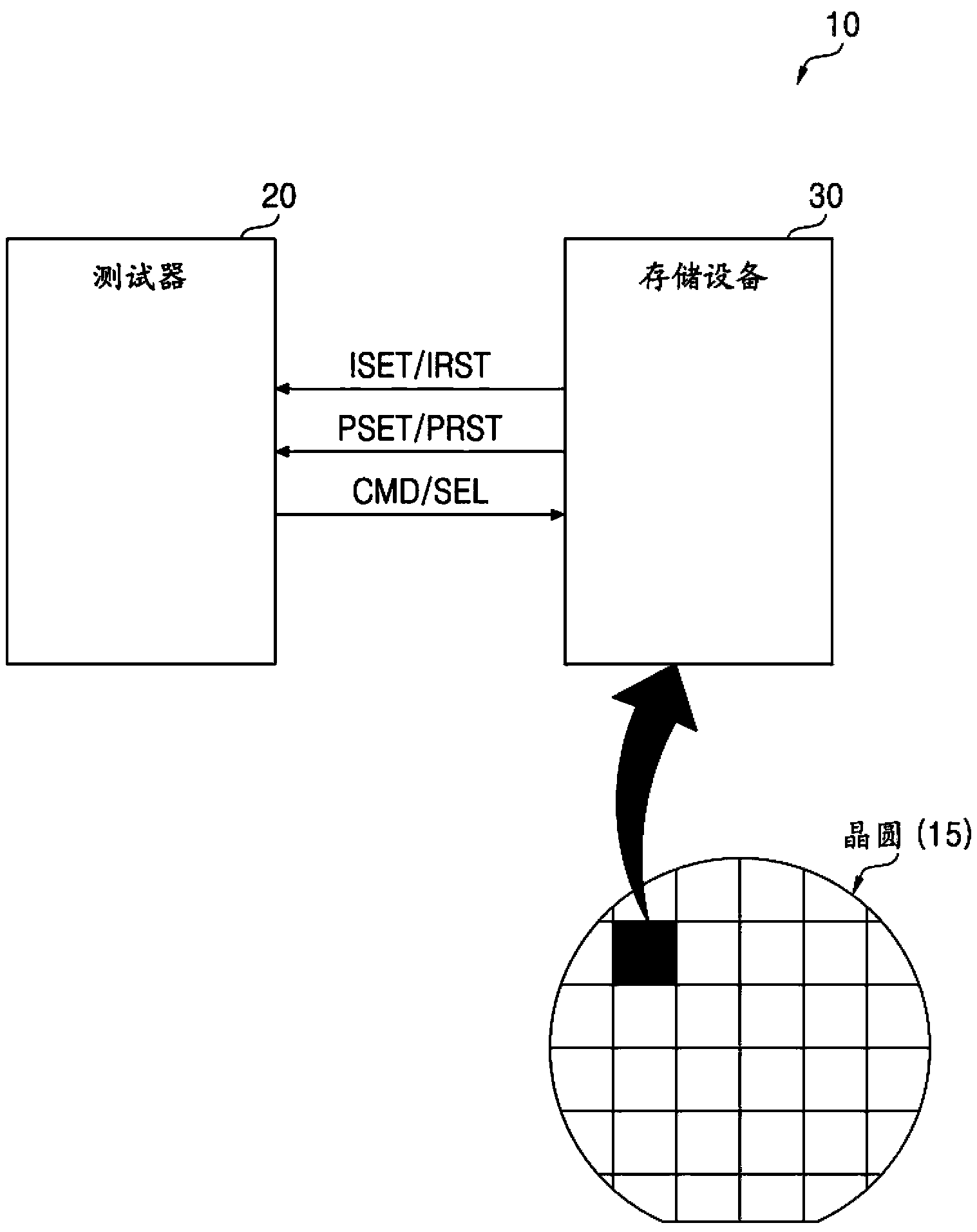
[0039] figure 1 is a block diagram of the system 10 for explaining a method of programming a delay for a nonvolatile memory device 30 according to an exemplary embodiment. Throughout the specification, "exemplary" means an example or illustration. Also, in this specification, "programmed delay" refers to the amount of delay used in adjusting the generation timing of a set pulse and / or the generation timing of a reset pulse generated based on one of a plurality of pulses included in a set pulse. , delay duration, or delay information.
[0040] refer to figure 1 , the system 10 includes a tester 20 and a non-volatile storage device 30 . The tester 20 is configured to test the performance of the nonvolatile memory device 30 . From the perspective of the tester 20 , the nonvolatile memory device 30 may be, for example, a device under test (DUT), and the DUT may be a chip included in the wafer 15 indicated by a shaded area. The non-volatile memory device 30 may be, for example...
PUM
 Abstract
Description
Claims
Application Information
 - R&D
- Intellectual Property
- Life Sciences
- Materials
- Tech Scout
- Unparalleled Data Quality
- Higher Quality Content
- 60% Fewer Hallucinations
Browse by: Latest US Patents, China's latest patents, Technical Efficacy Thesaurus, Application Domain, Technology Topic, Popular Technical Reports.
© 2025 PatSnap. All rights reserved.Legal|Privacy policy|Modern Slavery Act Transparency Statement|Sitemap|About US| Contact US: help@patsnap.com