ion implantation method

An ion implantation and ion technology, applied in electrical components, semiconductor/solid-state device manufacturing, circuits, etc., can solve the problems of non-standard wafer electrical parameters and wafer resistance value deviation.

Active Publication Date: 2016-03-09
CSMC TECH FAB2 CO LTD
View PDF7 Cites 0 Cited by
  • Summary
  • Abstract
  • Description
  • Claims
  • Application Information

AI Technical Summary

Problems solved by technology

However, if the number of scanning implants is increased to reduce the problems caused by a single scanning failure, and the ion beam current is correspondingly reduced to ensure that the implant dose remains unchanged, it will usually cause the resistance value of the wafer to shift, which will cause the wafer electrical parameter out of specification

Method used


Image

  • ion implantation method

Examples


Embodiment Construction

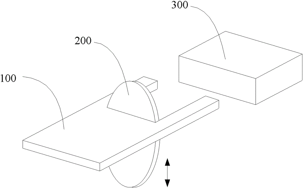
[0013] Such as figure 1 Shown is a schematic diagram of impacting a wafer with an ion beam. The ion beam 100 hits the wafer 200 to perform ion implantation on the wafer 200, and at the same time, the wafer 200 is driven by mechanical moving parts (not shown) to move back and forth in the vertical direction, so that the wafer 200 can be fully scanned, and after repeated times , the dose of ion implantation meets the requirements for making the resistance value of the wafer 200 reach the desired value.

[0014] On the side opposite to the emission of the ion beam 100, an ion beam current measuring device 300 is provided for providing data for monitoring the ion beam current. During the movement of the wafer 200 up and down, the shielded portion of the ion beam changes from less to more, and then to less, and so on. It is reflected on the ion beam current measuring device 300 that the detected current changes from large to small, then to large, and changes periodically.

[001...


PUM


Abstract

The invention discloses an ion implantation method which comprises the step of using an ion beam to beat a wafer. The wafer is driven by a mechanical moving part and is comprehensively scanned and beat by the ion beam repeatedly, and the ion beam current is 4 mA to 6.5 mA. The number of repeated and comprehensive beat of the wafer is determined according to implanted ion dosage and the ion beam current. Compared with the traditional ion implantation method, the ion current of the above ion implantation method is reduced, and the fact that the resistance value of the wafer is in an acceptable range of a normal value can be ensured. In addition, in the condition of same implantation dosage, the times of scanning implantation is increased correspondingly, the influence of the whole dosage by dosage reduction brought by single interference is relative small, and the possibility of disqualification of wafers is reduced.

Description

【Technical field】 [0001] The invention relates to a semiconductor manufacturing process, in particular to an ion implantation method. 【Background technique】 [0002] Ion implantation is a method of introducing controlled amounts of impurities into a silicon substrate to alter its electrical properties. The ion implanter emits an ion beam to impact the wafer to be implanted to dope the silicon wafer with a certain concentration of ions. [0003] During ion implantation, the current of the ion beam is kept constant, and the wafer is repeatedly moved several times so that the impact of the ion beam can cover the entire wafer. [0004] If the ion implantation machine interferes during the implantation process and causes the current of the ion beam to change, the ion dose of the scanning implantation will decrease. Under normal circumstances, when the current of the ion beam changes due to interference, the ion implantation should be stopped and the implantation position should...

Claims


Application Information

Patent Timeline
Patent Type & Authority Patents(China)
IPC IPC(8): H01L21/265
Inventor 李法涛
Owner CSMC TECH FAB2 CO LTD
Why Eureka
Try Eureka