

Semiconductor chip and package structure and method for forming same
A packaging structure and semiconductor technology, which is applied in the direction of semiconductor devices, semiconductor/solid-state device manufacturing, semiconductor/solid-state device components, etc., can solve problems such as time-consuming and labor-intensive, cost-increasing difficulties, and achieve the effect of overcoming time-consuming and labor-intensive effects
- Summary
- Abstract
- Description
- Claims
- Application Information
AI Technical Summary
Problems solved by technology
Method used
Image

Examples
Embodiment Construction
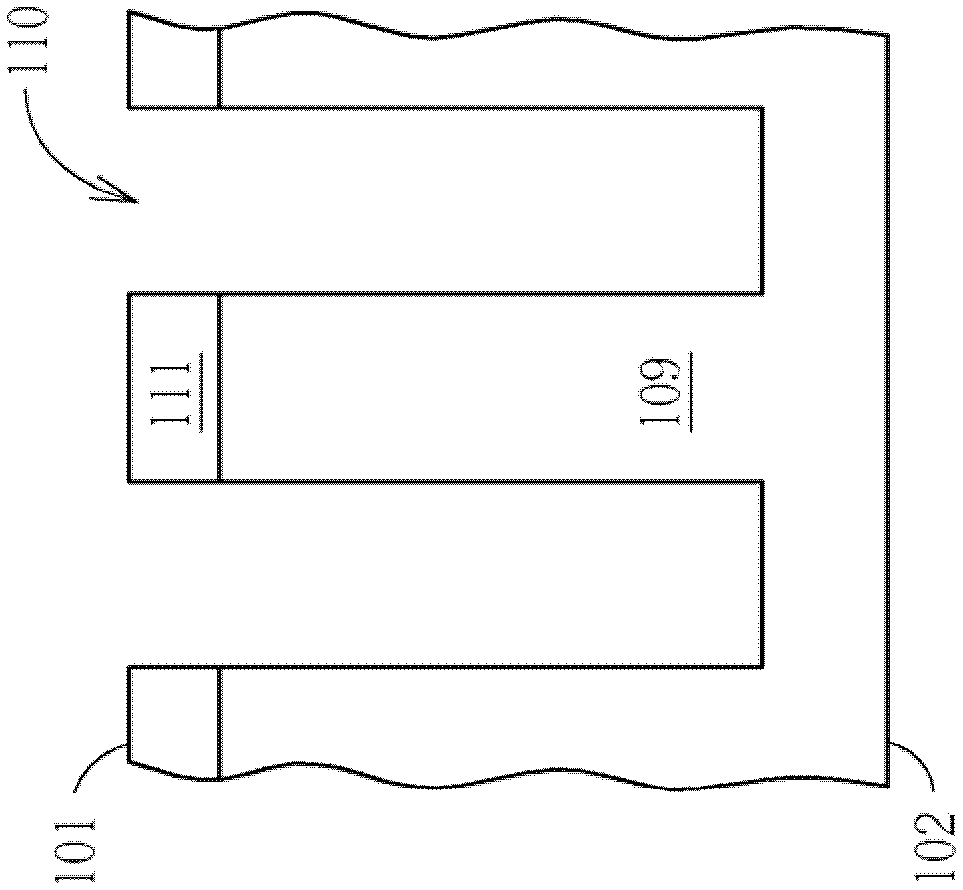
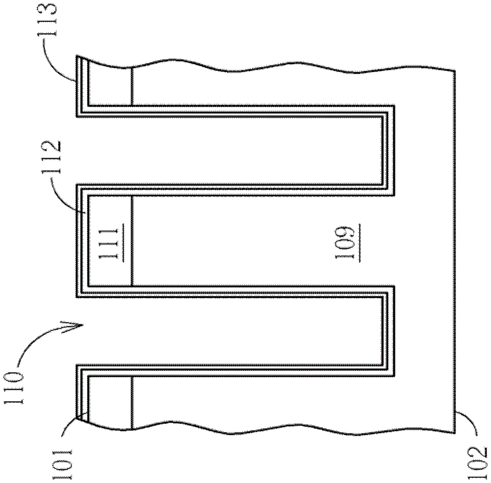
[0044] Figure 2 to Figure 6 Shown is a preferred embodiment of the present invention, illustrating a schematic diagram of the steps of forming the semiconductor chip of the present invention. Such as figure 2 As shown, firstly, a semiconductor substrate 109 is provided, including a first surface 101 and a second surface 102 . The semiconductor substrate 109 is, for example, a silicon substrate, an epitaxial silicon substrate, a silicon germanium semiconductor substrate, a silicon carbide substrate or a silicon-on-insulator (SOI) substrate, and has The first surface 101 and the second surface 102 . In a preferred embodiment of the present invention, the upper surface 101 is, for example, the active surface of the substrate 109 , and the lower surface 102 is, for example, the back surface of the substrate 109 . The upper surface 101 is opposite to the lower surface 102 . The thickness of the substrate 109 is generally 750 micrometers (micrometer), but not limited thereto. ...
PUM
 Abstract
Description
Claims
Application Information