Light emitting diode device

A technology of light-emitting diodes and electrodes, applied in electrical components, electrical solid-state devices, circuits, etc., can solve problems such as increased process time and cost, decreased internal quantum efficiency, and complex structures

Inactive Publication Date: 2013-10-30
PHOSTEK INC
View PDF4 Cites 0 Cited by
  • Summary
  • Abstract
  • Description
  • Claims
  • Application Information

AI Technical Summary

Problems solved by technology

However, such improved light-emitting diodes often result in complex structures (such as an increase in the number of epitaxial layers), thus increasing the process time and cost.
[0005]

Method used


Image

  • Light emitting diode device
  • Light emitting diode device
  • Light emitting diode device

Examples


Embodiment Construction

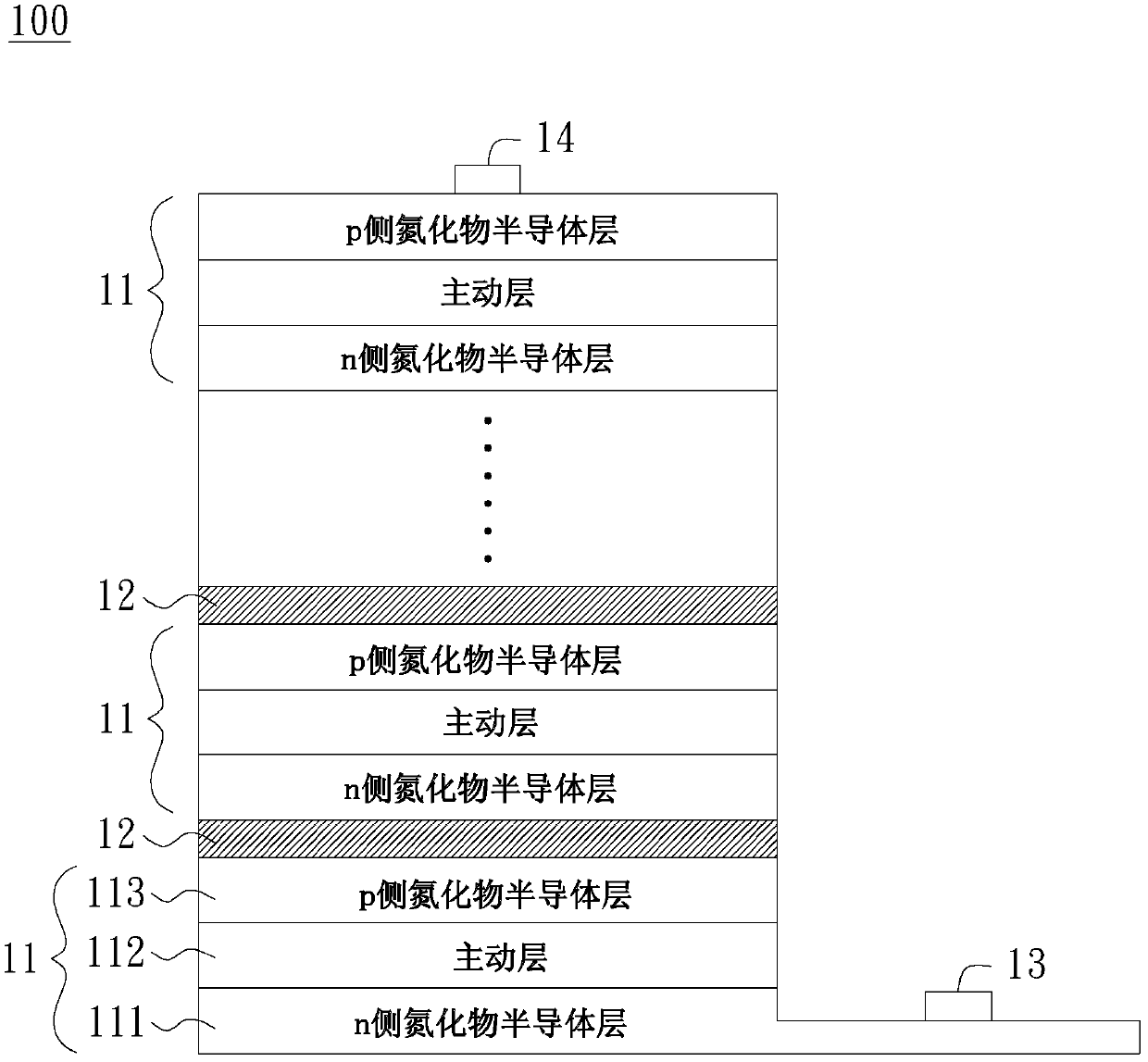
[0027] An embodiment of the invention discloses a light emitting diode (LED) device, which includes at least stacked LED units. figure 1 A cross-sectional view of a stacked LED unit 100 according to an embodiment of the present invention is shown, which includes a plurality of epitaxial structures 11 , and a tunnel junction 12 is formed between adjacent epitaxial structures 11 . Each tunnel junction 12 vertically stacks adjacent epitaxial structures 11 during the epitaxial process to form a stacked LED unit 100 . In this embodiment, the epitaxial structure 11 includes an n-side nitride semiconductor layer 111, an active layer 112 and a p-side nitride semiconductor layer 113, wherein the active layer 112 is between the n-side nitride semiconductor layer 111 and the p-side nitride semiconductor layer. Between layers 113. The tunnel junction 12 is located between the p-side nitride semiconductor layer 113 of one epitaxial structure 11 and the n-side nitride semiconductor layer 1...


PUM


Abstract

A light emitting diode device comprises at least one stack light emitting diode unit which is formed by stacking a plurality of epitaxial structures through tunnel junction faces. According to one characteristic of the light emitting diode device, for certain given preset input power, the stacked epitaxial structures enable the operation current density of the stack light emitting diode unit to be reduced to approach a quantum efficiency peak value. According to another characteristic of the light emitting diode device, for the certain given preset input power, the stack light emitting diode unit is operated in a current density section corresponding to the reduction degree within 20% of the quantum efficiency peak value.

Description

technical field [0001] The present invention relates to a light emitting diode device, in particular to a light emitting diode device with stacked light emitting diode units. Background technique [0002] Internal quantum efficiency (internal quantum efficiency, IQE) is a pointer commonly used to measure the luminous efficiency of light-emitting diodes (LEDs). proportion. General light-emitting diodes operate at low current densities (1-10A / cm 2 ) will correspond to a peak of internal quantum efficiency, representing the highest efficiency point. However, as the current density continues to increase, the efficiency will drop (droop). [0003] Considering the saving of chip area and cost reduction, and in order to achieve high-brightness light emission, traditional light-emitting diode devices do not operate at the highest efficiency point, but operate at a high current density of 30-50A / cm 2 Interval range. Because the efficiency of electricity-to-light conversion in th...

Claims


Application Information

Patent Timeline
IPC IPC(8): H01L27/15H01L33/38H01L33/04
Inventor 刘恒许进恭
Owner PHOSTEK INC
Why Eureka
Try Eureka