Light-emitting device and manufacturing method thereof

A technology for a light emitting device and a manufacturing method, which is applied in the direction of electrical components, circuits, semiconductor devices, etc., can solve the problems of reducing the uniformity and consistency of optical color performance, poor characteristics, and inability to uniformly mix light in a light emitting device 1, and achieve Solve the effects of poor color uniformity and consistency, good color uniformity and consistency, and good optical mixing effects

Inactive Publication Date: 2013-10-30
DELTA ELECTRONICS INC
View PDF5 Cites 9 Cited by
  • Summary
  • Abstract
  • Description
  • Claims
  • Application Information

AI Technical Summary

Problems solved by technology

[0004] Due to the material properties of the phosphor layer 14 (surface tension of the liquid, etc.) and the geometric relationship restrictions (such as a right-angle contact relationship) between the side surface of the light-emitting diode crystal grain 12 and the installation contact surface of the die adhesive portion 13, the phosphor powder layer 14 The part covering the side of the LED die 12 will have uneven thickness distribution, which will result in poor optical color mixed light character...

Method used


Image

  • Light-emitting device and manufacturing method thereof
  • Light-emitting device and manufacturing method thereof
  • Light-emitting device and manufacturing method thereof

Examples


Embodiment Construction

[0037] A light emitting device and its manufacturing method according to preferred embodiments of the present invention will be described below with reference to related drawings, wherein the same elements will be described with the same reference symbols.

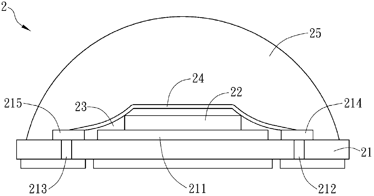
[0038] Please refer to figure 2 , which is a schematic diagram of a light emitting device according to a preferred embodiment of the present invention. The light emitting device 2 includes a substrate 21 , an LED die 22 , a first transparent layer 23 , a wavelength conversion layer 24 and a second transparent layer 25 . Wherein the substrate 21 has a die bonding portion 211, which is located at the center of the upper surface of the substrate 21, the LED die 22 is disposed on the die bonding portion 211, and the first transparent layer 23 covers the side of the LED die 22 and above, the light wavelength conversion layer 24 covers the first light transmission layer 23 with a uniform thickness, and the second light transmi...


PUM


Abstract

The invention discloses a light-emitting device and a manufacturing method of the light-emitting device. The light-emitting device comprises a substrate, a light emitting diode grain, a first light-pervious layer, a light wavelength conversion layer and a second light-pervious layer. The substrate is provided with a grain attachment portion, the light emitting diode grain is arranged on the grain attachment portion, the substrate is provided with a base, and the base is made of light-pervious materials. The first light-pervious layer covers the side face of the light emitting diode grain, the light wavelength conversion layer evenly covers the first light-pervious layer and the light emitting diode grain, and the second light-pervious layer covers the light wavelength conversion layer.

Description

technical field [0001] The invention relates to a light-emitting device and a manufacturing method thereof, in particular to a light-emitting device and a manufacturing method thereof suitable for a light-emitting diode crystal grain whose base is made of a light-transmitting material. Background technique [0002] One of the common light-emitting diode technologies at present is to use blue light-emitting diodes to excite yellow phosphors to achieve optical color mixing effects, and the optical performance of this technology is deeply affected by the state of phosphor coating in the process of packaging components of light-emitting diodes . [0003] Please refer to figure 1 , which is a schematic diagram of a conventional light-emitting device. The light-emitting device 1 includes a substrate 11 , LED die 12 , a die-attaching portion 13 , a phosphor layer 14 and a cover layer 15 . Wherein the die bonding part 13 is arranged in the center of the substrate 11, the light emi...

Claims


Application Information

Patent Timeline
IPC IPC(8): H01L33/50H01L33/52
Inventor 王宏洲陈绍尤刘家桦
Owner DELTA ELECTRONICS INC
Why Eureka
Try Eureka