Mask alignment device and photoetching device using same

A technology for mask alignment and support device, applied in the field of integrated circuit equipment manufacturing, can solve the problems of high cost, complex structure, and inability to obtain the drift amount in real time, and achieve the effect of reducing requirements

Active Publication Date: 2013-11-06
SHANGHAI MICRO ELECTRONICS EQUIP (GRP) CO LTD
View PDF5 Cites 14 Cited by
  • Summary
  • Abstract
  • Description
  • Claims
  • Application Information

AI Technical Summary

Problems solved by technology

[0004] Patent US4683572 provides a mask alignment device, the patent mask alignment sensor is located between the projection objective lens and the exposure object, and the mask alignment sensor is located outside the projection objective lens exposure field of view, so the patent has structural The following deficiencies: the projection objective lens is required to have a larger image-side working distance, which will lead to a complex design of the projection objective

Method used


Image

  • Mask alignment device and photoetching device using same
  • Mask alignment device and photoetching device using same
  • Mask alignment device and photoetching device using same

Examples


Embodiment approach

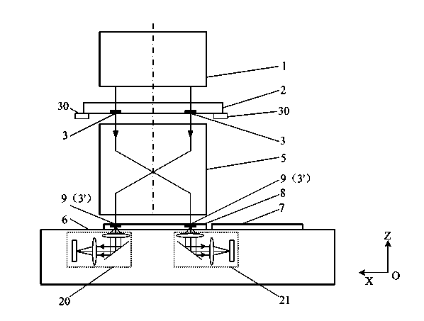
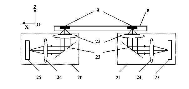
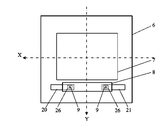
[0040] The present invention also provides a third preferred embodiment, which is as follows Figure 8 shown in. In this embodiment, the die alignment sensors 20 and 21 are arranged in the vertical direction, and the reflective surface is omitted in this embodiment.

[0041] Compared with the prior art, the mask alignment device provided by the present invention and the lithography apparatus using the device place the mask alignment sensor on the workpiece stage, thereby reducing the requirement for the working distance of the mirror image of the projection object, thereby reducing the projection The structure of the objective lens is complex and can effectively control the conjugate distance and weight of the projection objective lens.

[0042] Secondly, the mask alignment sensor can move with the workpiece stage into the exposure field of the projection objective, so the alignment light source can share the exposure light source when the mask marks are aligned, thereby redu...


PUM


Abstract

The invention discloses a mask alignment device and a photoetching device using same. The mask alignment device comprises 1, an illumination system for providing a light source to irradiate a first mark and a second mark, 2, a projection objective lens for imaging the first mark, 3, a first support device for supporting the first mark, wherein the first mark is located on a mask plate, 4, a second support device for supporting the second mark, wherein the second mark is located on a reference plate, and 5, an imaging detection system for detecting the deviation of a first mark imaging position and a second mark position. The mask alignment device is characterized in that the imaging detection system is fixed in the second support device; the second mark is located in a view field of the imaging detection system; and the projection objective lens and the imaging detection system use the illumination system in common.

Description

technical field [0001] The invention relates to the field of integrated circuit equipment manufacturing, in particular to a mask alignment device and a lithography apparatus using the same. Background technique [0002] The photolithography method refers to the circuit pattern drawn on the reticle, which is imaged on the surface of the silicon wafer for the manufacture of integrated circuits coated with photoresist and other photosensitive materials through a projection exposure device, and then the silicon wafer for the manufacture of integrated circuits is produced by an etching process. form a graph. Lithography equipment refers to equipment that uses photolithography to manufacture integrated circuits. The lithography equipment is to project and expose the circuit pattern on the reticle through an optical system such as a projection exposure lens, and project the circuit pattern on the silicon wafer for manufacturing the integrated circuit at a certain magnification or ...

Claims


Application Information

Patent Timeline
IPC IPC(8): G03F9/00G03F7/20
Inventor 徐兵周畅陈跃飞贾翔
Owner SHANGHAI MICRO ELECTRONICS EQUIP (GRP) CO LTD
Why Eureka
Try Eureka