Startup circuit and bandgap reference source circuit with startup circuit
A reference source circuit and start-up circuit technology, applied in the direction of adjusting electrical variables, control/regulating systems, instruments, etc., can solve problems such as the influence of the conduction voltage drop bandgap reference source circuit 10, so as to ensure normal operation and improve versatility Effect
- Summary
- Abstract
- Description
- Claims
- Application Information
AI Technical Summary
Problems solved by technology
Method used
Image

Examples
Embodiment 1
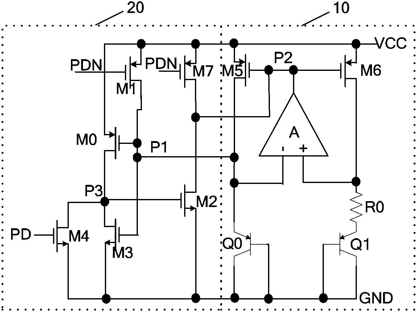
[0038] see image 3 , is a circuit diagram of Embodiment 1 of the bandgap reference source circuit including the start-up circuit of the present invention, the start-up circuit 200 is used to control the bandgap reference source circuit 100 to quickly enter the required working state after the circuit is started.
[0039] bandgap reference source circuit 100 with figure 1 The bandgap reference source circuit shown in is the same, including: PMOS transistors M5 and M6, operational amplifier A, bipolar transistor Q0 and Q1 resistor R0. Among them, the negative feedback circuit composed of PMOS transistors M5 and M6 and the operational amplifier A, the sources of the PMOS transistors M5 and M6 are connected to the voltage VCC, the drain of the PMOS transistor M5 and the emitter of the bipolar transistor Q0 are connected to the operational amplifier A The drain of the PMOS transistor M6 is connected to the non-inverting input of the operational amplifier A; the emitter of the bip...
Embodiment 2
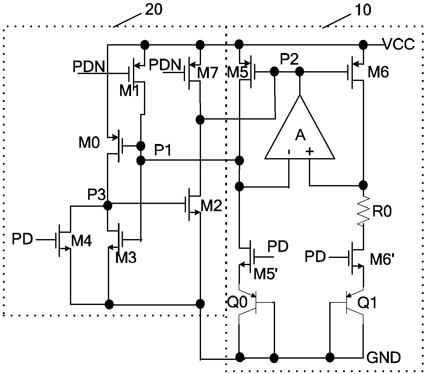
[0046] On the basis of Embodiment 1, a capacitive element can be added in the starting circuit, see Figure 4 , is the circuit diagram of Embodiment 2 of the bandgap reference source circuit including the start-up circuit of the present invention, the start-up circuit 201 is used to control the bandgap reference source circuit 100 to quickly enter the required working state after the circuit is started.
[0047] The start-up circuit 201 includes: three PMOS transistors, three NMOS transistors and a switch transistor, specifically the first PMOS transistor M7, the second PMOS transistor M0 and the third PMOS transistor M1, the first NMOS transistor M2, and the second NMOS transistor M3 and a third NMOS transistor M4, a switch transistor M8 and a capacitive element C0. Except for the capacitive element, other elements in the startup circuit 201 are the same as those in the startup circuit 200 in Embodiment 1, and will not be described here. The capacitive element is connected b...
Embodiment 3
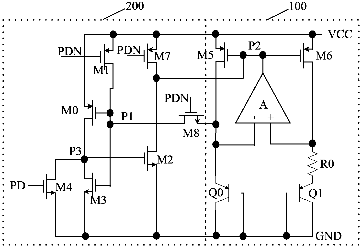
[0052] In the bandgap reference source circuit including the start-up circuit of the present invention, the switch tube may use bipolar transistors, such as NPN or PNP transistors.
[0053] see Figure 6 , in the bandgap reference source circuit including the start-up circuit in this embodiment, the start-up circuit 203 includes: three PMOS transistors, three NMOS transistors and a PNP transistor as a switch, specifically the first PMOS transistor M7, the second The PMOS transistor M0 and the third PMOS transistor M1, the first NMOS transistor M2, the second NMOS transistor M3 and the third NMOS transistor M4, and a PNP transistor M10 (switching transistor). Except for the PNP transistor M10 as a switch tube, other components in the start-up circuit 203 are the same as those in the start-up circuit 200 in Embodiment 1, and will not be repeated here. Wherein, the emitter of the PNP transistor M10 is connected to the gate of the second NMOS transistor M3, the collector is conne...
PUM
 Abstract
Description
Claims
Application Information
 - R&D
- Intellectual Property
- Life Sciences
- Materials
- Tech Scout
- Unparalleled Data Quality
- Higher Quality Content
- 60% Fewer Hallucinations
Browse by: Latest US Patents, China's latest patents, Technical Efficacy Thesaurus, Application Domain, Technology Topic, Popular Technical Reports.
© 2025 PatSnap. All rights reserved.Legal|Privacy policy|Modern Slavery Act Transparency Statement|Sitemap|About US| Contact US: help@patsnap.com