Preparation method of semiconductor substrate with cavity

A semiconductor and substrate technology, applied in the field of silicon-on-insulator substrate preparation, can solve problems such as inability to ensure uniformity, and achieve good top silicon uniformity and defect control effects

Active Publication Date: 2013-11-20
SHANGHAI SIMGUI TECH
View PDF2 Cites 17 Cited by
  • Summary
  • Abstract
  • Description
  • Claims
  • Application Information

AI Technical Summary

Problems solved by technology

[0003] Under the conventional BESOI thinning process, the top silicon thickness of Cavity-SOI is difficult to break through the limit of 5 μm, and good uniformity cannot be guaranteed; therefore, some SOI materials

Method used


Image

  • Preparation method of semiconductor substrate with cavity
  • Preparation method of semiconductor substrate with cavity
  • Preparation method of semiconductor substrate with cavity

Examples


Embodiment Construction

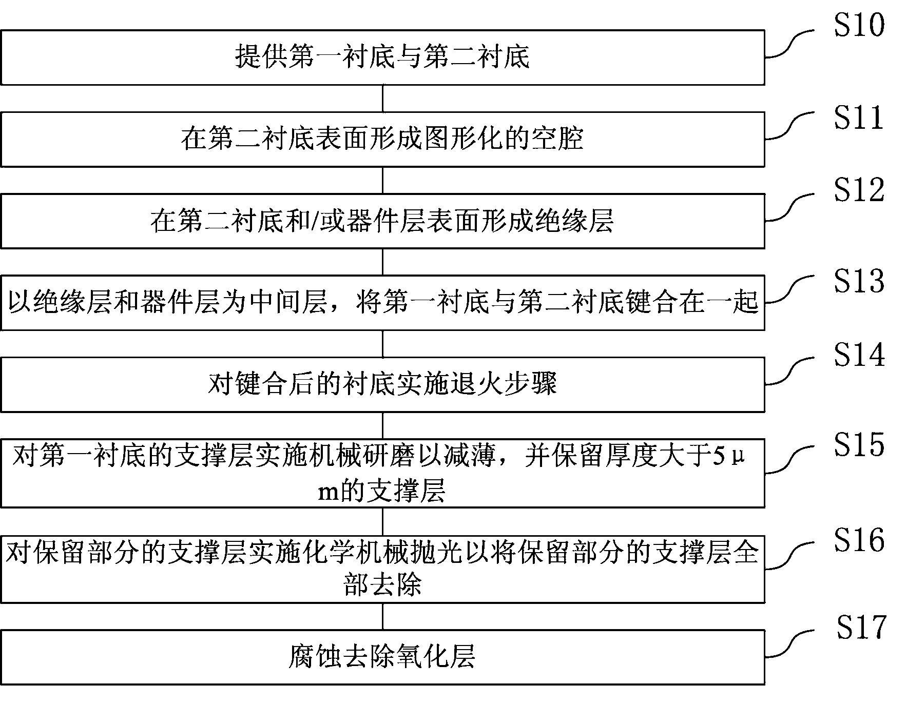
[0014] The specific implementation of the method for preparing a semiconductor substrate with a cavity provided by the present invention will be described in detail below in conjunction with the accompanying drawings.

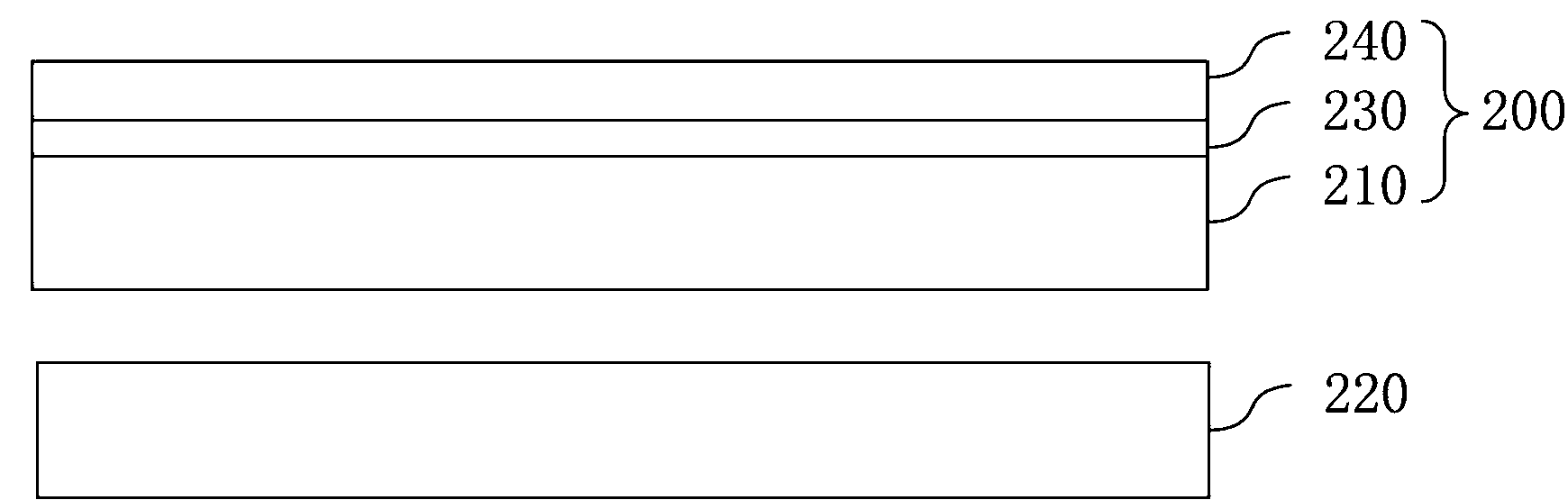
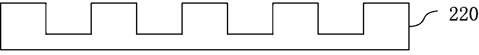
[0015] attached figure 1 Shown is a schematic diagram of the implementation of the steps of the method described in the specific embodiment of the present invention, including, step S10, providing a first substrate and a second substrate, the first substrate includes a support layer, an oxide layer on the surface of the support layer, and The device layer on the surface of the oxide layer; Step S11, forming a patterned cavity on the surface of the second substrate; Step S12, forming an insulating layer on the surface of the second substrate and / or the device layer; Step S13, forming the insulating layer and the device layer As an intermediate layer, the first substrate and the second substrate are bonded together; step S14, an annealing step is performed on the...


PUM

PropertyMeasurementUnit
Thicknessaaaaaaaaaa

Abstract

The invention provides a preparation method of a semiconductor substrate with a cavity. The preparation method comprises the following steps: a first substrate and a second substrate are provided, wherein the first substrate comprises a support layer, an oxidation layer on the surface of the support layer and a device layer on the surface the oxidation layer; the graphical cavity is formed on the surface of the second substrate; an insulating layer/insulating layers is/are formed on the surface/surfaces of the second substrate or/and the device layer; the first substrate and the second substrate are bonded together by taking the insulating layer and the device layer as middle layers; the annealing is performed on the bonded substrate; the mechanical lapping is performed on the support layer of the first substrate so as to reduce the thickness of the support layer, and the support layer with the thickness more than 5 um is reserved; the chemically mechanical polishing is performed on the support layer of a reserved part so as to completely remove the support layer of the reserved part; the oxidation layer is removed through corrosion so as to form semiconductor substrate with the cavity. The preparation method has the advantage that the combination method of the mechanical lapping, the chemically mechanical polishing and the corrosion is adopted, so that the crush of a top layer and a silicon layer due to only partial support during the process of mechanical lapping is prevented.

Description

technical field [0001] The invention relates to a method for preparing a silicon-on-insulator substrate, in particular to a method for preparing a semiconductor substrate with a cavity. Background technique [0002] The MEMS processing technology of silicon microstructure absorbs and integrates other processing technologies to realize various micromechanical structures. With the development of MEMS technology, Cavity-SOI material (silicon on insulator with cavity) has been used more and more in MEMS devices such as pressure sensors and gyroscopes. Bonding and Backside Thinning (BESOI) technology is currently the most mature and commercialized SOI technology: two oxidized silicon wafers are used as the support substrate and the device substrate respectively, and then bonded together at a temperature higher than 1000 ° C. Reinforce at high temperature for more than 2 hours, and then use grinding, polishing, etc. to thin the device substrate to the thickness required by the SO...

Claims


Application Information

Patent Timeline
IPC IPC(8): H01L21/762
Inventor 叶斐马乾志王中党
Owner SHANGHAI SIMGUI TECH
Why Eureka
Try Eureka