Static discharge clamping circuit with bias circuit in 90 nanometer CMOS (complementary metal-oxide-semiconductor transistor) process

A technology of electrostatic discharge and bias circuit, which is applied in the field of electrostatic discharge clamping circuit and electrostatic discharge protection, can solve the problems of large static leakage of RC network, and achieve the reduction of static leakage, reduction of capacitor area, increase, etc. The effect of effective resistance

Active Publication Date: 2013-11-20
XIDIAN UNIV
View PDF4 Cites 7 Cited by
  • Summary
  • Abstract
  • Description
  • Claims
  • Application Information

AI Technical Summary

Problems solved by technology

However, the effect of simply replacing the original capacitor with two capacitors in series to improve the static leakage is not obvious, and the problem of large static leakage of the RC network still occurs

Method used


Image

  • Static discharge clamping circuit with bias circuit in 90 nanometer CMOS (complementary metal-oxide-semiconductor transistor) process
  • Static discharge clamping circuit with bias circuit in 90 nanometer CMOS (complementary metal-oxide-semiconductor transistor) process
  • Static discharge clamping circuit with bias circuit in 90 nanometer CMOS (complementary metal-oxide-semiconductor transistor) process

Examples


Embodiment Construction

[0021] The present invention will be further described below with reference to the accompanying drawings and the embodiments thereof.

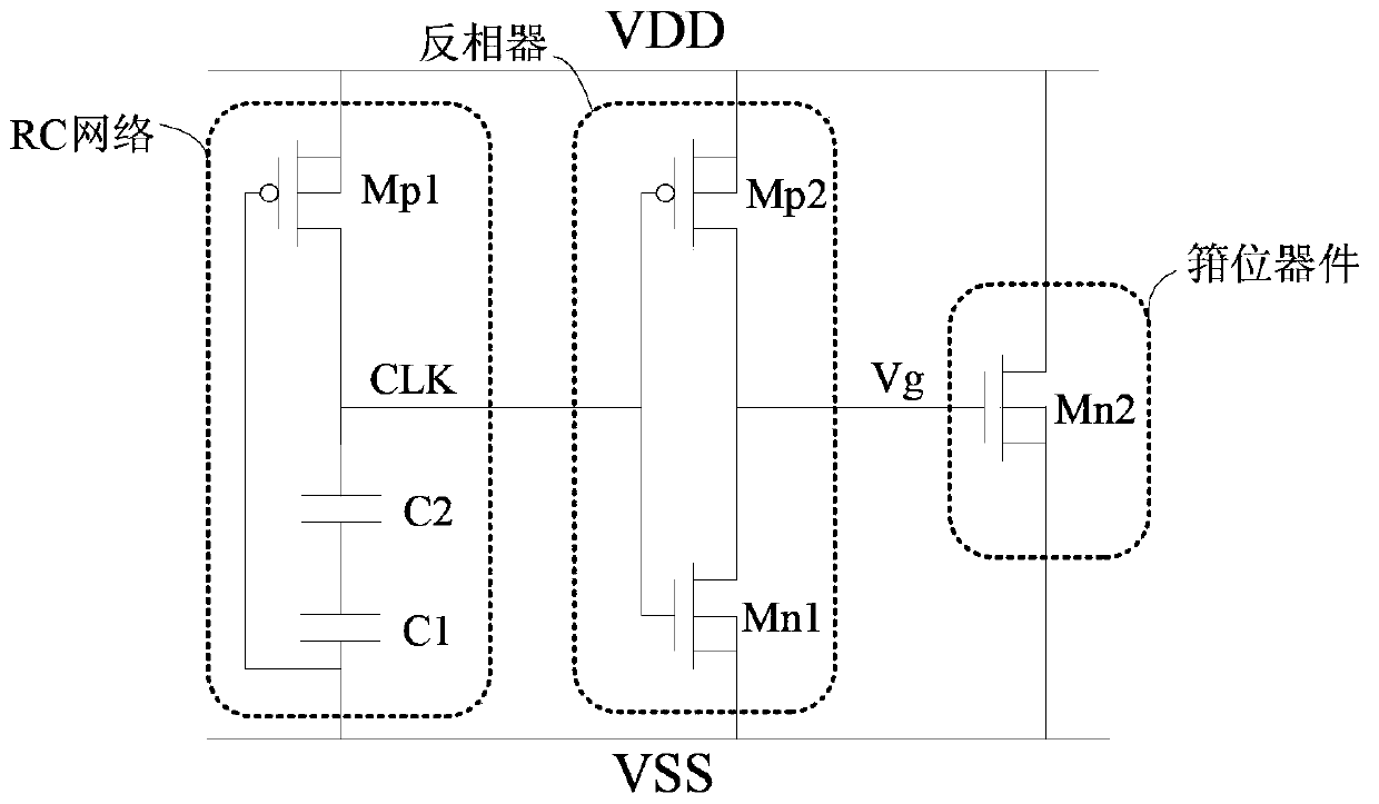
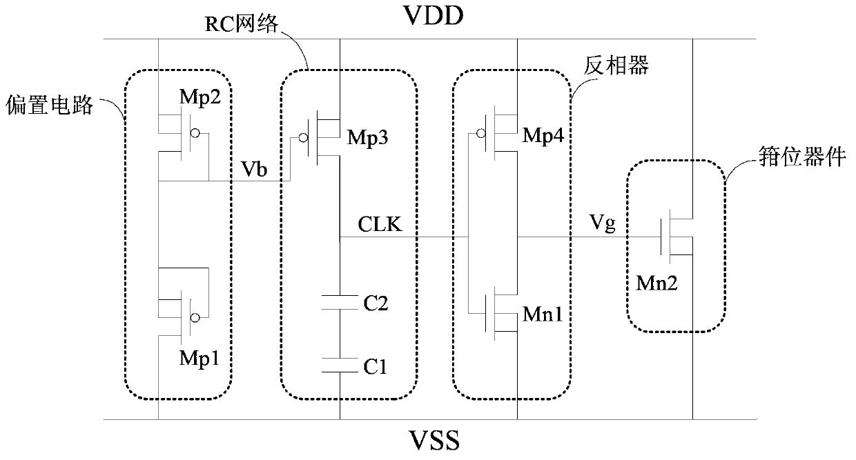
[0022] refer to figure 2 , the present invention includes: RC network, inverter, clamping device and bias circuit; Wherein:

[0023] The RC network includes: a first capacitor C1, a second capacitor C2 and a third PMOS transistor Mp3; one end of the first capacitor C1 is connected to one end of the second capacitor C2, and the other end of the first capacitor C1 is connected to the ground voltage VSS , the other end of the second capacitor C2 is connected to the drain of the third PMOS transistor Mp3; the third PMOS transistor Mp3 is used as a resistor, its source is connected to the power supply voltage VDD, its gate is connected to the bias voltage Vb, and its drain The pole is connected to the second capacitor C2, and the detection voltage CLK is input to the inverter for detecting electrostatic discharge.

[0024] The inverter includes:...


PUM


Abstract

The invention discloses a static discharge clamping circuit with a bias circuit in a 90 nanometer CMOS (complementary metal-oxide-semiconductor transistor) process. The static discharge clamping circuit mainly solves the problem of great RC (resistance-capacitance) network static electricity leakage in the static discharge clamping circuit in the existing 90 nanometer CMOS process. The circuit comprises an RC network, a phase inverter, a clamping device and a bias circuit, wherein the bias circuit provides bias voltage Vb of a grid electrode for a PMOS (P-channel metal oxide semiconductor) tube Mp3 in the RC network, as the bias voltage Vb is high voltage, the source grid voltage of the PMOS tube Mp3 is reduced, the equivalent resistance is increased, and the static electricity leakage of the RC network is reduced; during the static discharge, after the bias RC network detects the static discharge, the detection voltage CLK is input into the phase inverter, after the phase inverter receives the detection voltage, the grid electrode driving voltage Vg is input into the clamping device for starting the clamping device, and the static discharge charges are discharged. The static discharge clamping circuit has the advantages that the energy efficiency of the static discharge clamping circuit in the 90 nanometer CMOS process is improved, and the static discharge clamping circuit can be used for the design of integrated circuits.

Description

technical field [0001] The invention belongs to the technical field of electronic circuits and relates to electrostatic discharge protection, in particular to an electrostatic discharge clamping circuit with a bias circuit in a 90nm CMOS process, which can be used in integrated circuit design. Background technique [0002] During the manufacturing, packaging, transportation and use of integrated circuits, various forms of electrostatic discharge events are likely to occur. ESD events are characterized by instantaneous large stress and are one of the main failure modes of integrated circuits. ESD events cannot be completely avoided, so ESD protection must be considered when designing and manufacturing integrated circuits. The intensity of an electrostatic discharge event can be equivalent to a voltage. For example, in the human body model, the equivalent voltage of an electrostatic discharge event where electric sparks can be seen is generally as high as 3kV or more. The an...

Claims


Application Information

Patent Timeline
Patent Type & Authority Applications(China)
IPC IPC(8): H01L23/60
CPCH01L2924/0002H01L2924/00
Inventor 刘红侠杨兆年
Owner XIDIAN UNIV
Why Eureka
Try Eureka