Resilient printed circuit board pad structure

A technology for printed circuit boards and pads, which is applied in the directions of printed circuit components, electrical connection printed components, etc., can solve the problems of uneven pads, entering them, inconvenient cleaning, etc., and achieves the effect of improving the reliability of electrical connections

Active Publication Date: 2013-11-20
ANHUI BOTAI CIRCUIT TECH
View PDF5 Cites 5 Cited by
  • Summary
  • Abstract
  • Description
  • Claims
  • Application Information

AI Technical Summary

Problems solved by technology

At present, in common multi-layer printed circuit boards, there are usually pads, circuit layers and insulating layers from top to bottom, wherein the pads are located on the upper surface of the circuit layer, and the insulating layer is formed with through holes. Sometimes, the position of the pads It will correspond to the position of the through hole, and part or all of it will fall into the through hole. In this case, the processing of the pad will be unreliable, and it is easy to cause false soldering due to unevenness and collapse of the pad, resulting in electrical failure of the printed circuit board. Poor connection reliability; It should be pointed out that the support structure under the pad sometimes causes glue, ink, dust, etc. to enter it due to insufficient sealing, and it is not easy to clean

Method used


Image

  • Resilient printed circuit board pad structure

Examples


Embodiment Construction

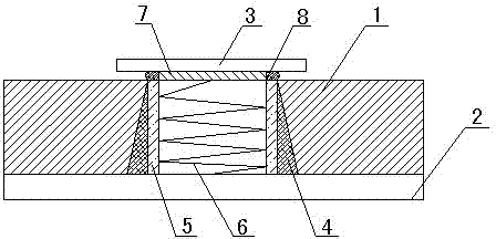
[0014] like figure 1 As shown, the flexible pad structure of the printed circuit board according to the embodiment of the present invention includes an insulating layer 1 and a base 2. The insulating layer 1 is arranged above the base 2, and a pad 3 is arranged on the top at the center of the insulating layer 1, located at A through hole is provided in the insulating layer 1 below the pad 3, and a triangular reinforcing rib 4 is respectively provided on both sides of the through hole, and a conductive layer 5 is provided on the inner side of each triangular reinforcing rib 4;

[0015] The spring assembly 6 is arranged inside the closed chamber surrounded by the conductive layer 5, the upper surface of the spring assembly 6 is connected to the pressure plate 7 and the upper surface of the pressure plate 7 is pressed against the lower bottom surface of the pad 3, and it is located on the outer edge of the pressure plate 7 and in the pad 3 and the conductive layer 5 are additiona...


PUM


Abstract

The invention discloses a resilient printed circuit board pad structure, which comprises an insulating layer and a base, the insulating layer is arranged on the top of the base, a pad is arranged on the top of the center of the insulating layer, the insulating layer is provided with a through hole under the pad, moreover, two triangular reinforcing ribs are respectively arranged on both sides of the inside of the through hole, the inner side of each triangular reinforcing rib is provided with a conductive layer, a spring assembly is arranged in the closed cavity defined by the conductive layers, and a holddown is connected with the top of the spring assembly. The resilient printed circuit board pad structure has the beneficial effects that: pad processing can become reliable, pseudo soldering as the result of the unevenness and sinking of the pad can be prevented, and thereby the reliability of the electric connection of a printed circuit board is enhanced; by adding the triangular reinforcing ribs, the pad structure is reinforced; and supporting force can be provided for the top pad from the bottom for a long time.

Description

technical field [0001] The invention relates to the field of printing technology, in particular to an elastic pad structure of a printed circuit board. Background technique [0002] Printed circuit boards have developed from single-layer boards to double-sided boards, multi-layer boards, and flexible boards, and are constantly developing in the direction of high precision, high density, and high reliability, continuously reducing volume, reducing costs, and improving performance. The development trend of printed circuit board manufacturing technology is to develop in the direction of high density, high precision, fine aperture, thin wire, small pitch, high reliability, multi-layer, high-speed transmission, light weight and thin shape in terms of performance. The wires of the single-sided panel only appear on one side, and the double-sided panel is an extension of the single-sided panel, which can conduct the lines between the two layers through the via holes to form the requ...

Claims


Application Information

Patent Timeline
Patent Type & Authority Applications(China)
IPC IPC(8): H05K1/11
Inventor 吴伟平
Owner ANHUI BOTAI CIRCUIT TECH
Why Eureka
Try Eureka