LCD panel, display device and manufacturing and driving methods of LCD panel and display device
A technology of liquid crystal panel and liquid crystal layer, which is applied in the field of display device and its manufacturing and driving, and liquid crystal panel, can solve the problems of affecting the optical display characteristics of products, uneven transmittance of display panel, poor distribution and the like
- Summary
- Abstract
- Description
- Claims
- Application Information
AI Technical Summary
Problems solved by technology
Method used
Image
Examples
Embodiment 1
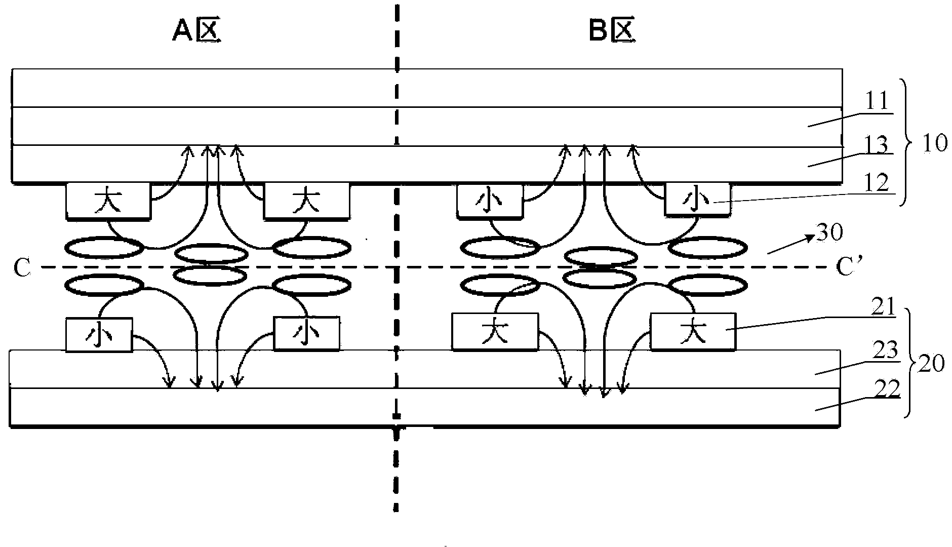
[0062] Such as figure 2 As shown, the embodiment of the present invention provides a liquid crystal panel, including an array substrate 20, a color filter substrate 10, and a liquid crystal layer 30 disposed between the two substrates. The array substrate 20 is provided with a first electrode 21 and a second electrode in different layers. 22. The third electrode 12 and the fourth electrode 11 are arranged in different layers on the color filter substrate 10, the first electrode 21 and the third electrode 12 are arranged opposite to each other, the first electrode 21 and the third electrode 12 are slit-shaped electrodes, and the second The electrode 22 and the fourth electrode 11 are plate-shaped electrodes, and the first electrode 21 and the third electrode 12 are respectively located on the side of the second electrode 22 and the fourth electrode 11 close to the liquid crystal layer 30 .
[0063] After the color filter substrate 10 and the array substrate 20 are aligned, the...
Embodiment 2
[0078] An embodiment of the present invention provides a liquid crystal panel, which is different from Embodiment 1 in that, refer to figure 2 As shown, a passivation layer 23 is provided between the first electrode 21 and the second electrode 22 on the array substrate 20, and a second passivation layer is provided between the third electrode 12 and the fourth electrode 11 on the color filter substrate 10. layer 13; and, the second passivation layer 13 on the color filter substrate 10 and the second passivation layer 23 on the array substrate have the same material and manufacturing process parameters, and are processed by the same equipment, so that the second The second passivation layer 13 has the same trend as the poor distribution of the passivation layer 23 (mainly the change in the thickness of the passivation layer). After the box is aligned, the poor distribution of the second passivation layer 13 and the passivation layer 23 is the opposite. (For the box-to-box mode...
Embodiment 3
[0080] An embodiment of the present invention provides a liquid crystal panel, which is different from Embodiment 1 in that, refer to figure 2 As shown, the fourth electrode 11 and the second electrode 22 of the array substrate 20 have the same material and manufacturing process parameters, and are processed by the same equipment, so that the prepared fourth electrode 11 has the same characteristics as the second electrode 22. Consistent distribution of bad trends, after pairing boxes such as figure 2 As shown, making the poor distribution trend of the fourth electrode 11 and the second electrode 22 is opposite, can compensate the difference in electric field distribution caused by the poor distribution of the process parameters of the first electrode 21 and the second electrode 22, and improve the display effect of the product.
PUM
 Abstract
Description
Claims
Application Information


