Single SOC chip and multi-working mode multiplexing method of single SOC chip

A working mode and chip technology, applied in the fields of instruments, electrical digital data processing, etc., can solve the problems of not being able to close the SOC chip, the SOC chip cannot be configured, and the on-chip interconnection bus configuration connection, etc., to reduce research and development risks and costs, The effect of shortening R&D cycle and time-to-market of chips

Active Publication Date: 2013-11-27
INST OF COMPUTING TECH CHINESE ACAD OF SCI
View PDF5 Cites 18 Cited by
  • Summary
  • Abstract
  • Description
  • Claims
  • Application Information

AI Technical Summary

Problems solved by technology

[0013] In addition, there are currently some SOC chip design schemes that also support multiple working modes for a single SOC chip. A combination of quantity, speed, or type has three major limitations on configurable parameters: first, the on-chip interconnect bus in the SOC chip cannot be configured to connect (such as the common AMBA bus) to the chip pins, nor That is to say, the SOC chip cannot be configured as a processor core IP Testchip chip; secondly, even if the SOC chip contains an external interconnection bus module, it still works in bridge mode and cannot be configured to

Method used


Image

  • Single SOC chip and multi-working mode multiplexing method of single SOC chip
  • Single SOC chip and multi-working mode multiplexing method of single SOC chip
  • Single SOC chip and multi-working mode multiplexing method of single SOC chip

Examples


Embodiment Construction

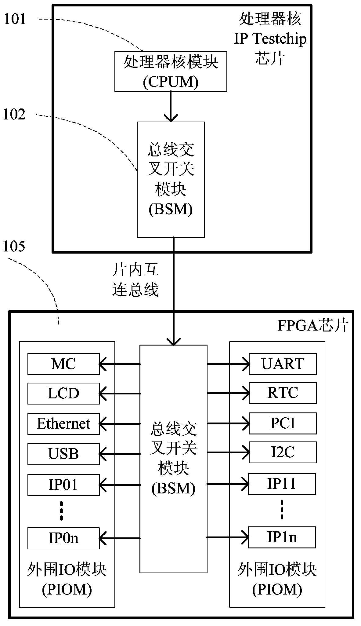
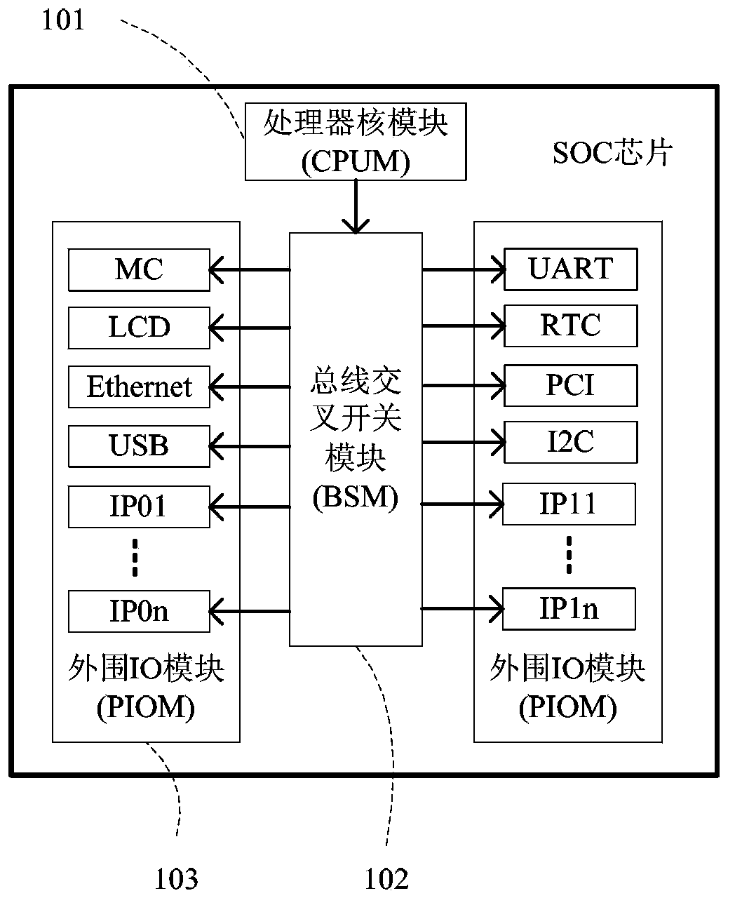
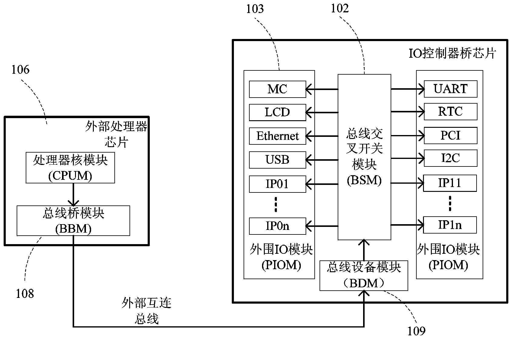
[0044] The multi-mode single SOC chip disclosed by the present invention includes a processor core module (CPUM), a mode control module (MCM), a function enabling module (FEM), a bus crossbar switch module (BSM), a pin control module (PCM), External Interconnect Bus Module (EIBM), Peripheral IO Module (PIOM), Auxiliary Function Module (AFM).

[0045] in,

[0046] 1. Processor core module (CPUM): used to interpret instructions and process data.

[0047] The CPUM of the chip is the computing and control core of the entire chip. Generally, the CPU is composed of an arithmetic unit, a controller, registers, and a bus that realizes the data, control, and status of their connections.

[0048] 2. Mode control module (MCM): used to control the working mode of the chip.

[0049] During the power-on reset period of the chip, the MCM sends control signals to the function enable module, the bus crossbar switch module, the pin control module, and the external interconnection bus module a...


PUM


Abstract

The invention relates to a single SOC (System On Chip) chip and a multi-working mode multiplexing method of the single SOC chip. The single SOC chip comprises a central processor core module and a peripheral IO module and further comprises a mode control module, a function enabling module, a bus crossbar switch module, an external interconnection bus module, a pin control module and an auxiliary functional module. The mode control module is used for controlling the working modes of the single SOC chip, and the working modes of the single SOC chip comprise a central processor core IP (Intellectual Property) test chip mode, an SOC chip mode and an IO controller bridge chip mode. The function enabling module is used for selecting functional modules needing to be starting up or shutting down. The bus crossbar switch module is used for selecting the address space mapping manners of the functional modules; the external interconnection bus module is used for determining whether the single SOC chip works in the bridge mode or the device mode. The pin control module is used for controlling the IO pin of the single SOC chip to be connected to a signal bus in the single SOC chip. The auxiliary functional module is used for turning on/off the clock and power supply of the functional modules. According to the invention, a manufacturer of the single SOC chip only needs to design one type of tape-out chip to meet three application requirements of the market. Therefore, the frequency of the tape-out chip design is reduced from three times to once, the research and development cycle and the time to market of the conventional single SOC chips are shortened, and the research and development risk and cost of the conventional single SOC chip are lowered.

Description

technical field [0001] The invention relates to the technical field of integrated circuits, in particular to a single SOC chip and a method for multiplexing multiple working modes of the single SOC chip. Background technique [0002] A system on a chip (SOC) is an integrated circuit that integrates a computer or other electronic systems onto a single chip. The SOC chip generally consists of a central processing unit (abbreviated as CPU), a memory controller core (memory controller, abbreviated as MC), an intellectual property core (abbreviated as IP) for other input and output interfaces, and other auxiliary function modules such as A clock phase-locked loop core (phase-locked loops, abbreviated as PLL) and a voltage planning controller core (voltage regulator, abbreviated as VR) are composed. [0003] SOC is generally used in embedded systems. It is based on a single chip and a small number of discrete peripheral devices such as memory chips to form a complete computer sys...

Claims


Application Information

Patent Timeline
IPC IPC(8): G06F13/36
Inventor 吴少校苏孟豪
Owner INST OF COMPUTING TECH CHINESE ACAD OF SCI
Why Eureka
Try Eureka