Storage unit, forming method of storage unit and driving method of storage unit

A memory cell and control gate technology, applied in the semiconductor field, can solve the problems of occupying a large area and low memory integration, and achieve the effects of improving the integration, reducing the number of use, and reducing the chip area

Active Publication Date: 2013-11-27
SHANGHAI HUAHONG GRACE SEMICON MFG CORP
View PDF4 Cites 17 Cited by
  • Summary
  • Abstract
  • Description
  • Claims
  • Application Information

AI Technical Summary

Problems solved by technology

But this causes the selection control transistor to occupy a larger area in the memory device, making the memory less integrated

Method used


Image

  • Storage unit, forming method of storage unit and driving method of storage unit
  • Storage unit, forming method of storage unit and driving method of storage unit
  • Storage unit, forming method of storage unit and driving method of storage unit

Examples


Embodiment Construction

[0020] As mentioned in the background art, each group of gates of the existing EEPROM cells corresponds to at least one selection control transistor, so that the selection control transistor occupies a larger area of ​​the memory chip.

[0021] In order to increase the integration level of the memory chip, it is necessary to reduce the number of select control transistors without affecting various read, write and erase operations on the memory cells.

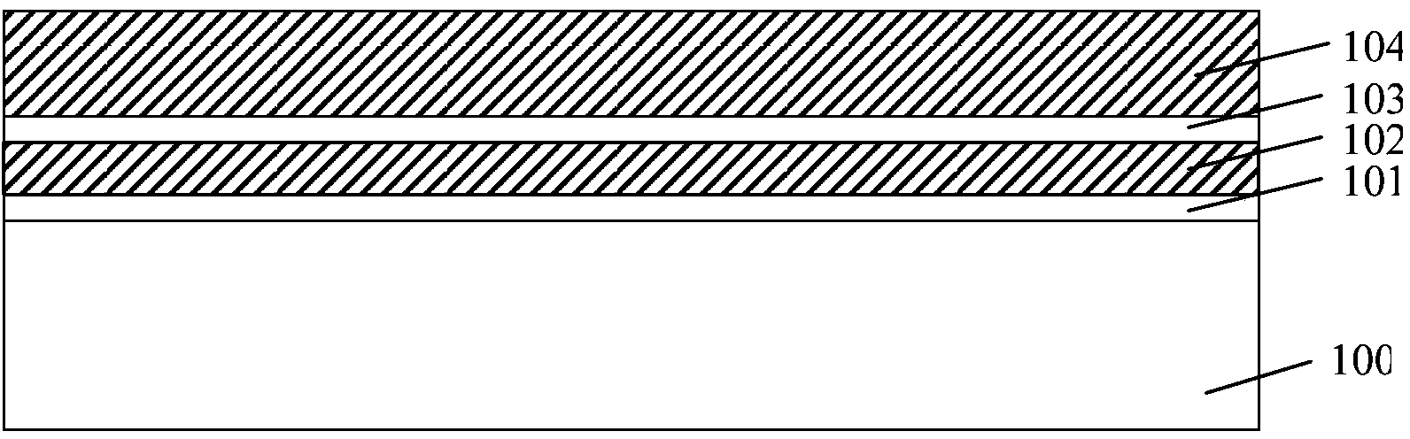
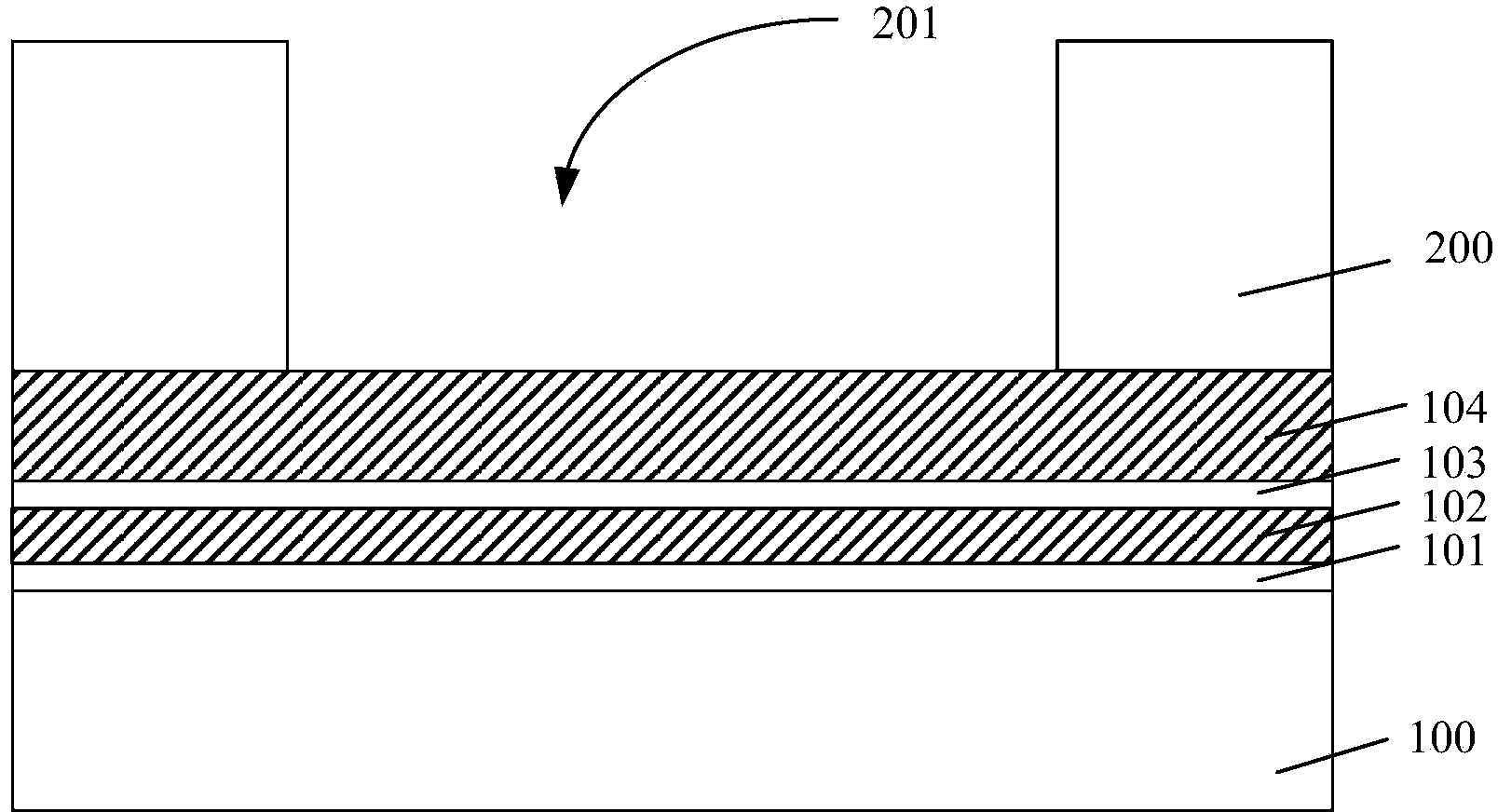
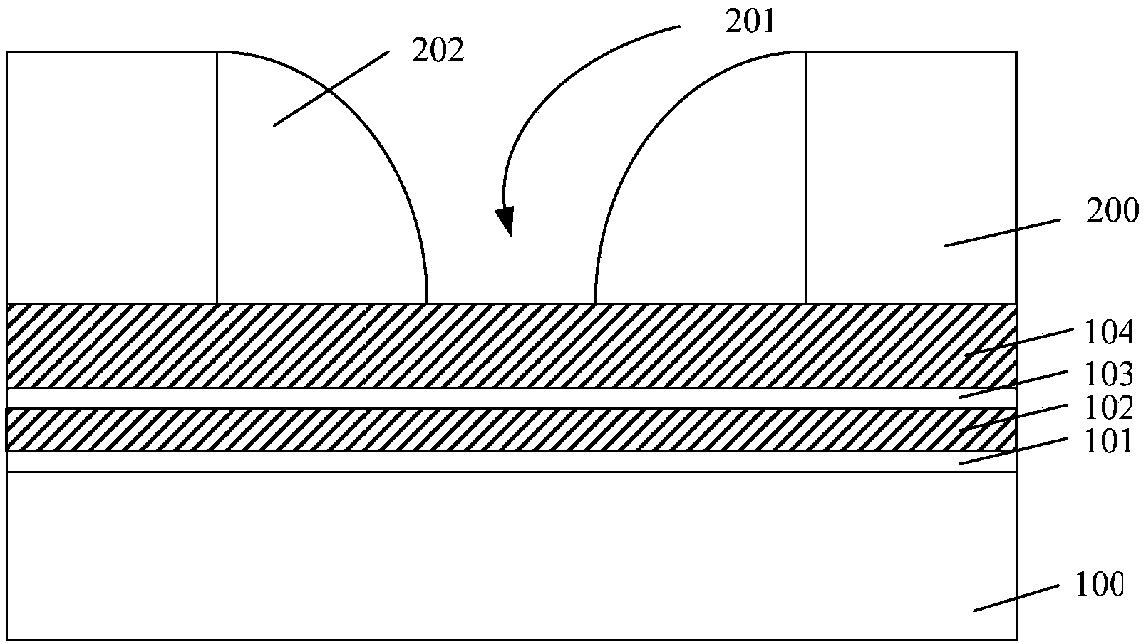
[0022] In order to solve the above problems, the source and drain of the memory cell formed in the embodiment of the present invention are located under the floating gate dielectric layer, which improves the coupling rate between the floating gate and the source or drain, so that the drain or The source voltage controls the opening or closing of the channel under the floating gate, so that the control gates on both sides of the word line are connected to the same selection control transistor to still realize the reading, writing ...


PUM


Abstract

The invention provides a storage unit, a forming method of the storage unit and a driving method of the storage unit. The forming method of the storage unit includes the steps that a semiconductor substrate is provided, and a first dielectric layer, a floating gate material layer, a second dielectric layer, a control gate material layer and a mask layer are formed on the surface of the semiconductor substrate; a first side wall is formed on the surface of the side wall of an opening; the control gate material layer is etched to form a first groove; a second side wall is formed; the second dielectric layer, the floating gate material layer and the first dielectric layer are etched to form a second groove; a tunneling oxidation layer is formed on the surface of the inner wall of the second groove; word lines are formed on the surface of the tunneling oxidation layer; a first control gate, a first control gate dielectric layer, a first floating gate, a first floating gate dielectric layer, a second control gate, a second control gate dielectric layer, a second floating gate and a second floating gate dielectric layer are formed; source electrodes and drain electrodes are formed. According to the storage unit formed by the forming method, the two control gates can be controlled only by one control transistor, therefore, the number of selected transistors can be effectively reduced, and the integration level of a storage is improved.

Description

technical field [0001] The present invention relates to the technical field of semiconductors, in particular to a storage unit, a method for forming the same, and a method for driving the storage unit. Background technique [0002] In the current semiconductor industry, integrated circuit products can be mainly divided into three types: logic, memory and analog circuits, among which storage devices account for a considerable proportion of integrated circuit products, such as RAM (random access memory), DRAM (dynamic Random access memory), ROM (read-only memory), EPROM (erasable programmable read-only memory), FLASH (flash memory) and FRAM (ferroelectric memory), etc. [0003] The development of flash memory devices in memory is particularly rapid. Its main feature is that it can keep the stored information for a long time without power on. It has many advantages such as high integration, fast access speed and easy erasure, so it has been widely used in many fields such as m...

Claims


Application Information

Patent Timeline
Patent Type & Authority Applications(China)
IPC IPC(8): H01L21/8247H01L27/115G11C16/06
Inventor 于涛
Owner SHANGHAI HUAHONG GRACE SEMICON MFG CORP
Why Eureka
Try Eureka