Substrate/multi-chip-integrated large port interconnection chip and realization method thereof

A technology of multi-chip integration and implementation method, which is applied in the field of substrate multi-chip integrated large-port interconnect chips and its implementation, can solve the problems of chip area, chip power consumption, chip cost, and integrated circuit manufacturing capacity limitations, and achieve improved scalability. The effect of high reliability, low production cost and low cost

Active Publication Date: 2013-11-27
INST OF COMPUTING TECH CHINESE ACAD OF SCI
View PDF10 Cites 19 Cited by
  • Summary
  • Abstract
  • Description
  • Claims
  • Application Information

AI Technical Summary

Problems solved by technology

[0014] In order to solve the scalability of the above-mentioned single-chip integrated large-port interconnection chips, which are limited by chip area, chip power consumption, chip cost, and integrated circuit manufacturing capabilities, the present invention proposes a multi-chip integration based on multi-layer wiring substrates. , large-port interconnect chip interconnection construction and physical implementation method

Method used


Image

  • Substrate/multi-chip-integrated large port interconnection chip and realization method thereof
  • Substrate/multi-chip-integrated large port interconnection chip and realization method thereof
  • Substrate/multi-chip-integrated large port interconnection chip and realization method thereof

Examples


Embodiment Construction

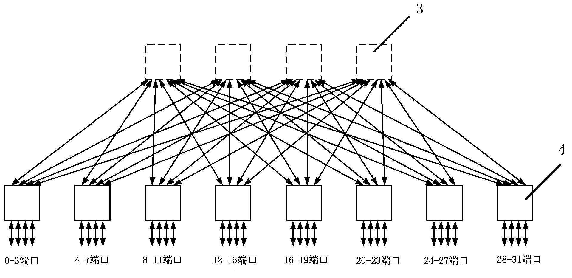
[0063] In order to effectively solve the problem that the number of integrated ports of single-chip large-port interconnection chips is severely limited, the present invention proposes a multi-layer wiring substrate, multi-chip integration, large-port interconnection chip interconnection structure and corresponding physical realization. method. Compared with the corresponding single-chip integration method, the present invention can support multiple interconnection structures, and has better balance in terms of chip implementation cost, scalability, flexibility, compatibility, etc. The requirements for integrated circuit manufacturing technology are lower, and substrate-integrated large-port interconnection chips with different numbers of ports and different specifications can be provided at the same time, which is more flexible in adapting to market demand.

[0064] The technical solution of the present invention will be described in detail below.

[0065] Interconnect sub-c...


PUM


Abstract

The invention provides a multilayer wiring substrate/multi-chip integration-based large port interconnection chip interconnection construction and physical realization method and relates to a multi-chip interconnection structure, a multi-chip interconnection structure construction method, multi-chip layout, substrate pin array partitioning and distribution, distribution of high-speed differential signal pin pairs, effective partition of substrate wiring and a partition method of the substrate wiring as well as a corresponding multi-chip interconnection chip device which are applicable to substrate integration. According to the invention, large-port interconnection chips can be effectively and equivalently realized based on substrate encapsulation size. Compared with a corresponding single-chip integration implementation method, the method of the invention can support multiple kinds of interconnection structures, and is compatible with interconnection sub-chips be of a variety of micro-system structures, can effectively utilize the characteristics of different functional interconnection sub-chips, and has better performance in implementation cost of the chips, scalability, flexibility, compatibility and the like; and at the same time, the method of the invention has lower requirements for manufacturing technology for realizing a required integrated circuit and can provide interconnection chips having different specifications and different number of ports, and can more flexibly adapt to market demands.

Description

technical field [0001] The present invention relates to a construction and physical realization method of a large-port interconnection chip using multi-layer wiring substrate and multi-chip integration technology, and relates to a multi-chip interconnection network system structure and construction method suitable for substrate integration, and a corresponding substrate Physical implementation methods such as internal multi-chip interconnection structure, multi-chip layout, substrate metal pin array division, high-speed differential signal pair pin assignment, substrate wiring area division, and corresponding multi-chip interconnection chip devices based on substrate integration. Background technique [0002] The interconnection network structure and interconnection chips play an important role in high-performance computer systems, and are one of the key factors that determine the overall performance, scalability, and cost of the system. In order to build a large-scale compu...

Claims


Application Information

Patent Timeline
Patent Type & Authority Applications(China)
IPC IPC(8): H01L23/485H01L23/50H01L23/52H01L21/768
CPCH01L2224/16225H01L2924/15192H01L2924/15311
Inventor 沈华曹政孙凝晖张佩珩元国军安学军游定山杨佳解利伟
Owner INST OF COMPUTING TECH CHINESE ACAD OF SCI
Why Eureka
Try Eureka