Semiconductor luminescent device for improving luminous efficiency and manufacturing method thereof

A technology of light-emitting devices and luminous efficiency, applied in semiconductor devices, electric solid-state devices, electrical components, etc., can solve the problems of reducing light output rate and light loss, increase heat conduction effect, increase electrical conductivity, and reduce the probability of collapse Effect

Inactive Publication Date: 2013-11-27
GUANGDONG SHENLAITE SCI & TECH
View PDF4 Cites 0 Cited by
  • Summary
  • Abstract
  • Description
  • Claims
  • Application Information

AI Technical Summary

Problems solved by technology

The light diffusely reflected in the chip groove will be absorbed by the silver glue, and the more the silver glue is used, the more obvious the absorbed light will be. Therefore, no matter increasing the silver content in the silver glue or increasing the amount of silver glue, it will cause the chip groove. The light is absorbed, causing light loss and reducing the light output rate

Method used


Image

  • Semiconductor luminescent device for improving luminous efficiency and manufacturing method thereof
  • Semiconductor luminescent device for improving luminous efficiency and manufacturing method thereof
  • Semiconductor luminescent device for improving luminous efficiency and manufacturing method thereof

Examples


Embodiment Construction

[0042] In order to make the object, technical solution and advantages of the present invention clearer, the present invention will be further described in detail below in conjunction with the accompanying drawings and embodiments. It should be understood that the specific embodiments described here are only used to explain the present invention, not to limit the present invention.

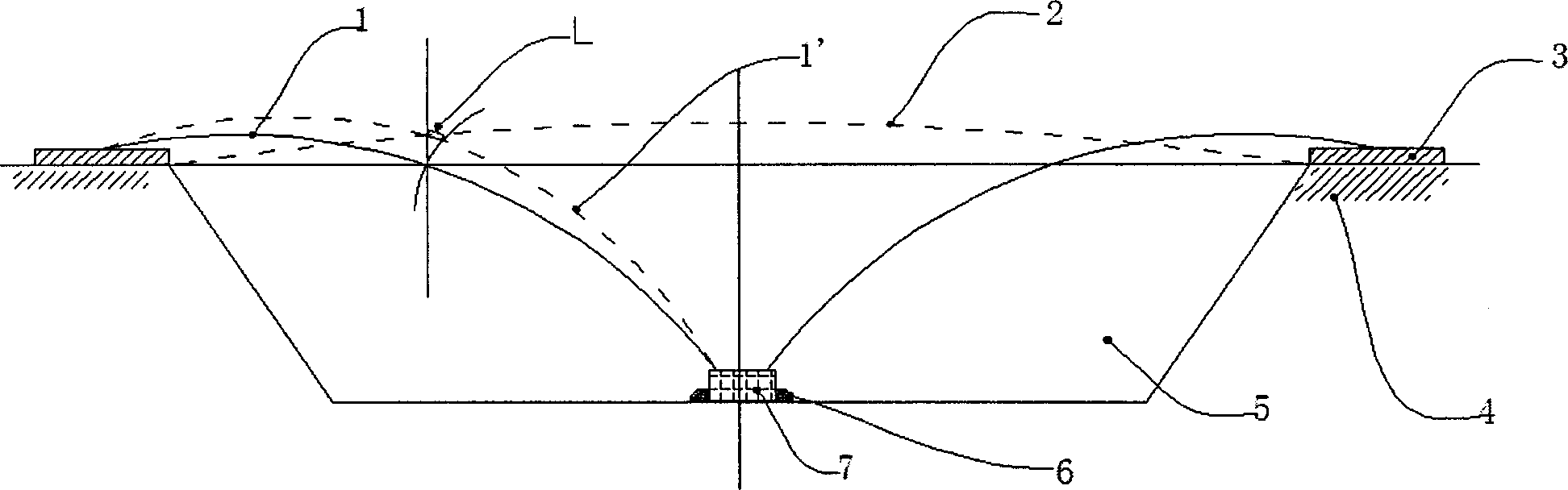
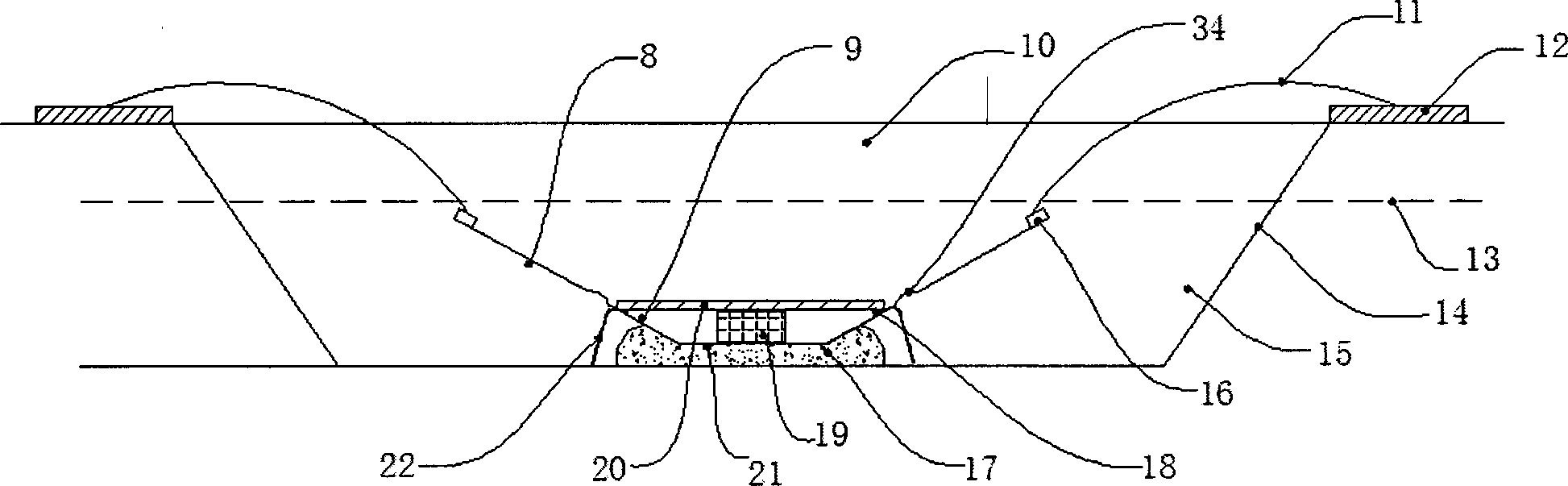
[0043] Figure 2 to Figure 8 As an embodiment of the present invention, the LED chip 19 is fixed in the chip slot 15 of the bracket. Electrode wires 12 are arranged on the bracket, and LED chips 19 are electrically connected to the electrode wires 12 through lead wires 11 . The LED chip 19 is fixed on the pressure dividing sheet 9, and the pressure dividing sheet 9 is fixed in the chip groove by the silver glue below it. The pressure divider 9 includes a bottom 21 and a lead lifting portion 8 connected to the bottom. In one embodiment, the lead lifting part has a certain inclination angle upward...


PUM


Abstract

The invention provides a semiconductor luminescent device for improving luminous efficiency and a manufacturing method thereof, and the semiconductor luminescent device and the manufacturing method thereof relate to the packaging technology of luminescent semiconductor, and are used for improving the light emitting rate and device performances. The technical scheme of the invention is that: an LED chip is fixed on the upper surface of a pressure dividing plate, and the pressure dividing plate is fixed in a chip groove; the pressure dividing plate comprises a bottom part and a lead lifting part; the bottom part comprises a light processing region and a die-bonding region arranged in the middle of the light processing region, and the light processing region forms an upwards tilt angle relative to the die-bonding region; the lower surface of the bottom part is provided with sliver glue; bending baffle plates are arranged at edges of the bottom part, the bending baffle plates separate the oblique space below the light processing region from the outside, so that the silver glue is surrounded by a group of bending baffle plates; the chip is a flip chip, and the surface thereof comprising a non-welding region on a flip-chip substrate is painted with an RGB fluorescent powder layer; and the surface of the light processing region is painted with an RGB fluorescent powder layer, layer structures under the RGB fluorescent powder layer include a single-primary-color fluorescent powder layer, and layer structures under the single-primary-color fluorescent powder layer include a reflective layer.

Description

technical field [0001] The invention relates to the packaging technology of light-emitting semiconductors. Background technique [0002] For the packaging methods of existing high-power LED light-emitting devices, see figure 1 scheme shown. The LED chip 7 is fixed in the chip groove 5 of the bracket 4 through the silver glue 6 . The lead wire 1 connects the electrode of the LED chip with the electrode wire 3 on the bracket. The LED chip is fixed in the chip groove by sealing glue. When this LED device is working, the internal junction temperature of the chip will exceed 100 degrees Celsius, and the temperature in the lamp cavity is also 70-90 degrees Celsius. The sealant in the chip slot is made of epoxy resin material as an example. When the lead wire is gold wire, the epoxy resin will have obvious thermal expansion and contraction under the temperature difference of tens of degrees, and the expansion coefficient of gold wire is only its Below one-fifth, it is not obvi...

Claims


Application Information

Patent Timeline
Patent Type & Authority Applications(China)
IPC IPC(8): H01L33/48H01L33/62H01L33/64H01L33/54H01L33/60H01L33/50
CPCH01L2224/48091H01L2224/73265H01L2924/19107H01L2924/00014
Inventor 冯海涛蔡德晟
Owner GUANGDONG SHENLAITE SCI & TECH
Why Eureka
Try Eureka