Formation method of semiconductor structure

A semiconductor and dielectric layer technology, applied in the field of semiconductor structure formation, can solve problems such as wafer deformation and semiconductor device failure, and achieve the effects of small superposition effect, reduced internal stress, and good release effect

Active Publication Date: 2018-09-07
SEMICON MFG INT (SHANGHAI) CORP
View PDF11 Cites 0 Cited by
  • Summary
  • Abstract
  • Description
  • Claims
  • Application Information

AI Technical Summary

Problems solved by technology

Since the thermal expansion coefficients of the metal interconnection layer and the dielectric material are very different, when the ambient temperature of the multilayer stacked metal interconnection structure changes greatly, the thermal internal heat suffered by the metal interconnection line and the dielectric material The stress difference is also very large, causing the internal stress migration (Stress Migration, SM) of the multi-layer stacked metal interconnection structure, which will cause the wafer to deform, and in severe cases, the semiconductor device will fail.

Method used


Image

  • Formation method of semiconductor structure
  • Formation method of semiconductor structure
  • Formation method of semiconductor structure

Examples


Embodiment Construction

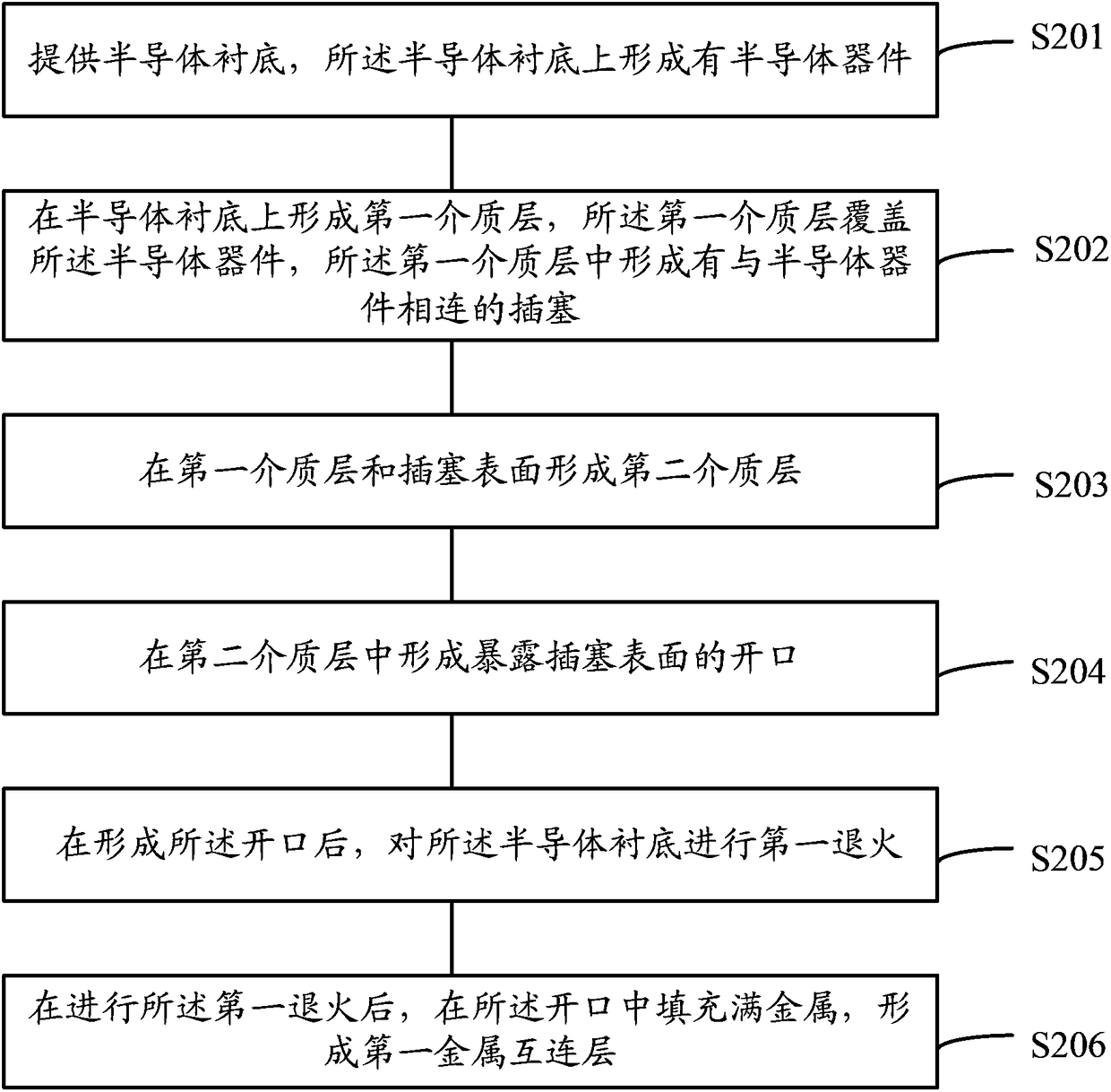
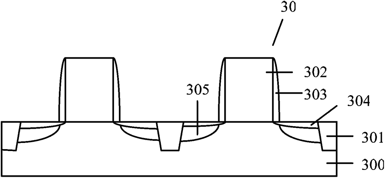
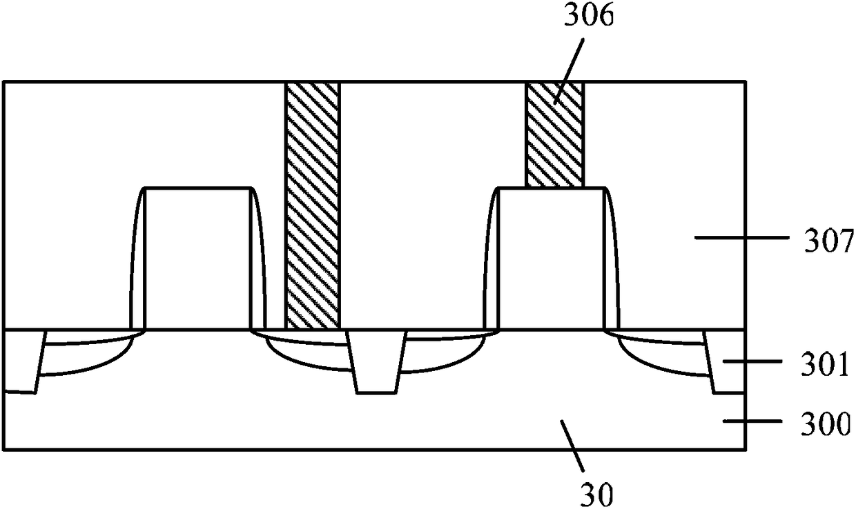
[0028] The inventor found in the process of back-end metal interconnection process that the back pressure (Backside Pressure BSK) of the physical vapor deposition equipment often shifted when processing the wafer, especially in the top-level metal interconnection process, it would occur The phenomenon that the back pressure suddenly decreases. The size of the back pressure reflects the control of the position of the backside of the wafer by the electric suction chuck in the physical vapor deposition equipment (normally 7~9Torr). The smaller the value of the back pressure, it means that the electric suction The worse the position control of the suction chuck for the wafer is, the wafer will tilt in the cavity after it is less than a certain set value (usually 5Torr). When the back pressure value deviates from the allowable value, it needs to be corrected Wafers are reworked, which is likely to lead to chipping. The inventors further researched and found that the deviation of th...


PUM


Abstract

A semiconductor structure forming method comprises the steps of providing a semiconductor substrate, wherein a semiconductor component is formed on the semiconductor substrate; forming a first medium layer on the semiconductor substrate, wherein the first medium layer covers the first semiconductor component, and a plug connected with the semiconductor component is formed in the first medium layer; forming second medium layers on the surface of the first medium layer and the surface of the plug; forming an opening exposing the surface of the plug in the second medium layer; after forming the opening, conducting first annealing on the semiconductor substrate; after conducting the first annealing, filling metal into the opening and forming a first metal mutual connecting layer. Before the first metal mutual connecting layer, the first annealing is conducted, so that inner stress between various materials on the semiconductor substrate is reduced, and the stacking effect of the inner stress is reduced after the first metal mutual connecting line is formed.

Description

technical field [0001] The invention relates to the field of semiconductor manufacturing, in particular to a method for forming a semiconductor structure. Background technique [0002] With the advancement of semiconductor technology, the size of integrated circuits has become smaller and smaller. When the integration of integrated circuits increases, the surface of the chip cannot provide enough area to make the required interconnection lines. Therefore, most of the current VLSI structures use a multi-layer stacked metal interconnection structure. [0003] In the multi-layer stacked metal interconnection structure, each layer of metal interconnection layer includes several metal interconnection lines, and the metal interconnection lines in the same layer are separated by dielectric materials, and the metal interconnection lines in different layers The wires are also separated by dielectric materials, and the metal interconnection wires of different layers are connected by ...

Claims


Application Information

Patent Timeline
Patent Type & Authority Patents(China)
IPC IPC(8): H01L21/324H01L21/768
Inventor 李广宁
Owner SEMICON MFG INT (SHANGHAI) CORP
Why Eureka
Try Eureka