Partially-depleted silicon-on-insulator device structure

A technology of silicon-on-insulator and device structure, which is applied in the manufacture of electric solid-state devices, semiconductor devices, semiconductor/solid-state devices, etc. It can solve problems such as uneven opening and affecting device performance, and achieve uniform parasitic resistance and improve uniformity.

Inactive Publication Date: 2013-12-11
SHANGHAI HUAHONG GRACE SEMICON MFG CORP
View PDF4 Cites 7 Cited by
  • Summary
  • Abstract
  • Description
  • Claims
  • Application Information

AI Technical Summary

Problems solved by technology

In the PDSOI MOSFET, due to the limited thickness of the gate 140, the parasitic resistance 190 of the body region 131 will make the dynamic threshold MOSFET turn on unevenly, thereby affecting the performance of the device

Method used


Image

  • Partially-depleted silicon-on-insulator device structure
  • Partially-depleted silicon-on-insulator device structure
  • Partially-depleted silicon-on-insulator device structure

Examples


Embodiment Construction

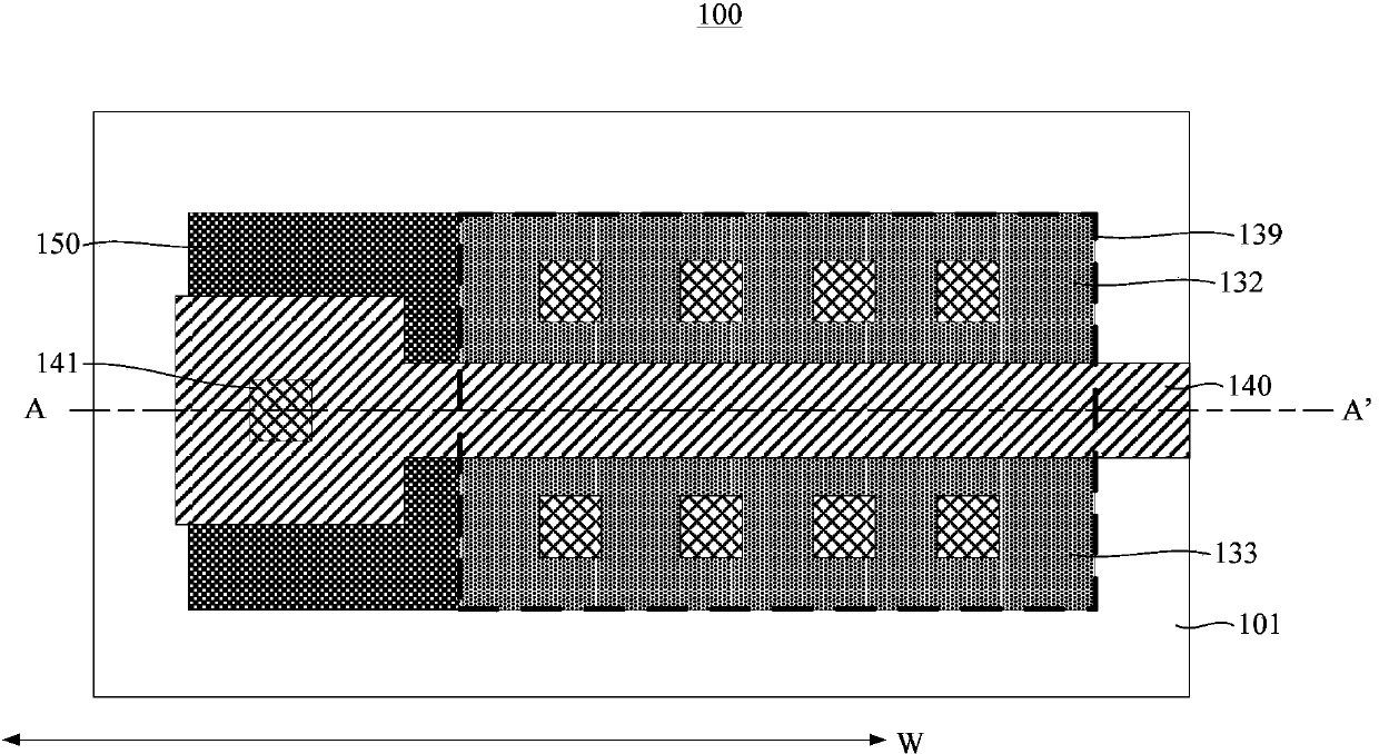
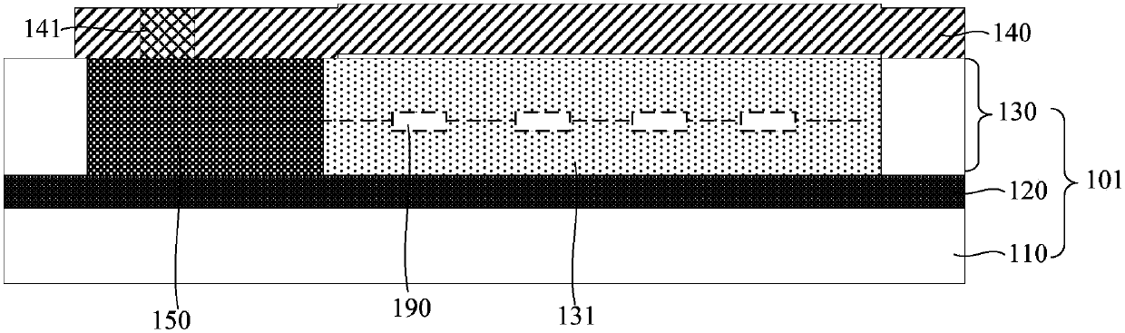
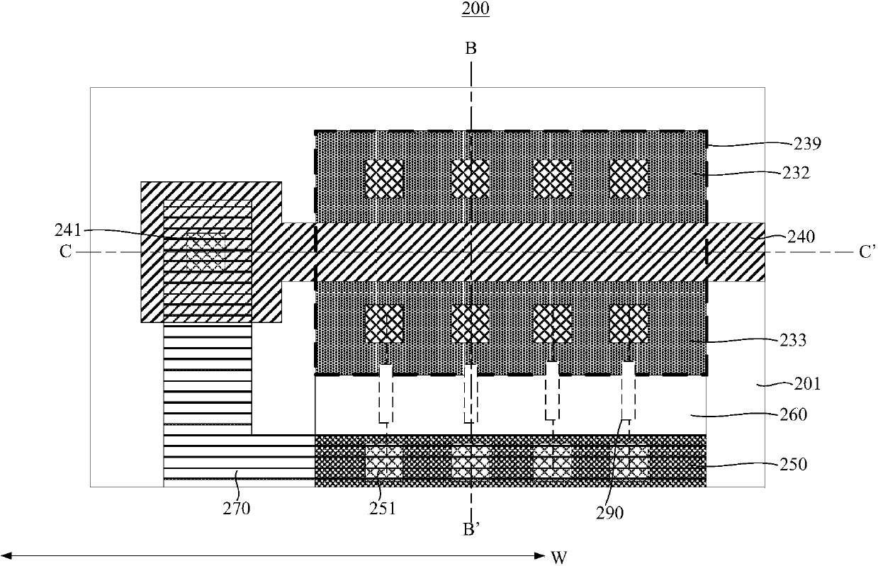
[0027] The structure of the partially depleted silicon-on-insulator device of the present invention will be described in more detail below in conjunction with schematic diagrams, wherein a preferred embodiment of the present invention is represented, and it should be understood that those skilled in the art can modify the present invention described herein while still implementing the present invention. Beneficial effects of the invention. Therefore, the following description should be understood as the broad knowledge of those skilled in the art, but not as a limitation of the present invention.

[0028] In the following paragraphs the invention is described more specifically by way of example with reference to the accompanying drawings. Advantages and features of the present invention will be apparent from the following description and claims. It should be noted that all the drawings are in a very simplified form and use imprecise scales, and are only used to facilitate and...


PUM


Abstract

The invention provides a partially-depleted silicon-on-insulator device structure. The partially-depleted silicon-on-insulator device structure comprises a semiconductor substrate, a device active area, a grid and a body contact active area. The semiconductor substrate comprises a bottom layer substrate, an insulation area buried layer and an upper layer substrate, wherein the bottom layer substrate, the insulation area buried layer and the upper layer substrate are sequentially stacked from bottom to top. The device active area is placed in the upper layer substrate and comprises a body region, a source region and a drain region. The grid stretches cross the device active area, the body region is placed below the grid, and the source region and the drain region are placed on the two sides of the grid respectively. The body contact active area is placed in the portion, on one side of the device active area in the width direction, of the upper layer substrate, the body contact active area is isolated from the drain region or the source region through a shallow insulation area, the shallow insulation area does not make contact with the insulation area buried layer, and the grid is electrically connected with the body contact active area. According to the partially-depleted silicon-on-insulator device structure, the evenness of starting of a partially-depleted silicon-on-insulator dynamic threshold transistor can be improved.

Description

technical field [0001] The invention relates to the technical field of semiconductor manufacturing, in particular to a partially depleted silicon-on-insulator device structure. Background technique [0002] In silicon on insulator (silicon on insulator, referred to as SOI) technology, the device is only manufactured in a thin silicon film on the surface, and the device is isolated from the underlying substrate by an oxide insulating region buried layer. The parasitic capacitance of this structure is small , so that the SOI device has the characteristics of high speed and low power consumption. Since the full dielectric isolation of SOI CMOS devices completely eliminates the parasitic latch-up effect of bulk silicon CMOS devices, SOI full dielectric isolation makes SOI technology have high integration density and good radiation resistance. Therefore, SOI technology is widely used in radio frequency, high voltage and anti-radiation. radiation etc. [0003] SOI MOS devices ar...

Claims


Application Information

Patent Timeline
Patent Type & Authority Applications(China)
IPC IPC(8): H01L27/12H01L21/762
Inventor 刘张李
Owner SHANGHAI HUAHONG GRACE SEMICON MFG CORP
Why Eureka
Try Eureka