

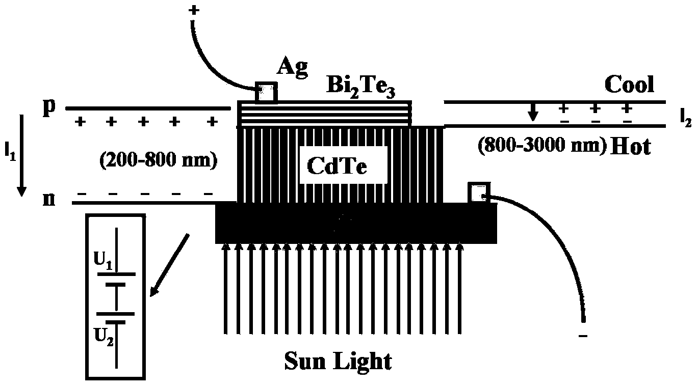
Cadmium telluride/bismuth telluride integrated nano structure material with photo-thermal synergic electric generation and preparation method thereof
A nanostructure, photothermal synergy technology, applied in the manufacture/processing of thermoelectric devices, metal material coating technology, circuits, etc., can solve the problems of reducing the efficiency of photovoltaic cells, and cannot really solve the problem of full-spectrum absorption and utilization of solar energy
- Summary
- Abstract
- Description
- Claims
- Application Information
AI Technical Summary
Problems solved by technology
Method used
Image

Examples
preparation example Construction
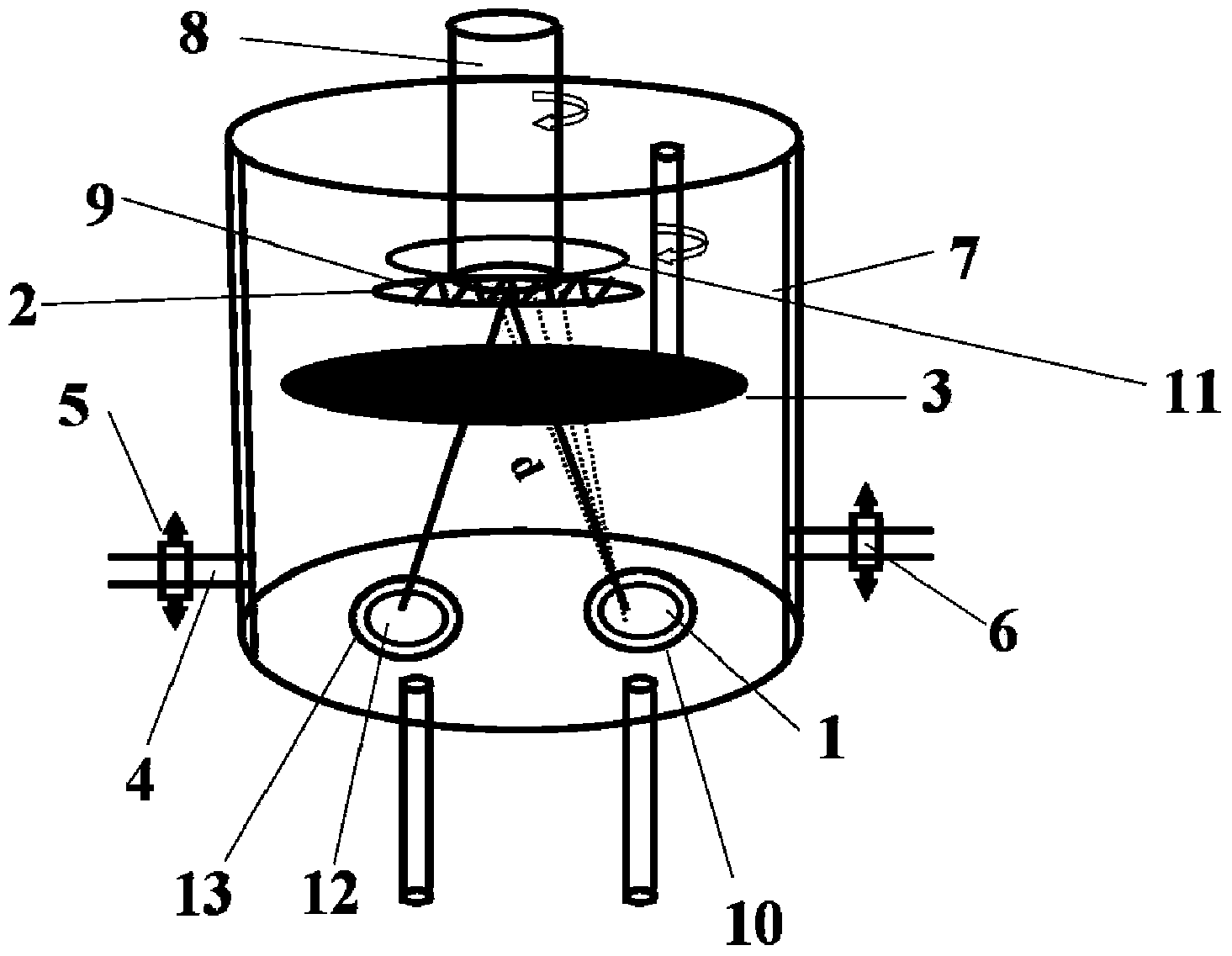
[0067] In the preparation method of the present invention, the distance d between the sample stage 2 and the radio frequency stage (sputtering source) 1, the sputtering pressure, the temperature of the substrate, and the size of the radio frequency power supply must be adjusted, and then the sputtering can be controlled to obtain the deposition on the conductive surface. The cadmium telluride nanowire array on the glass substrate makes the structure of the cadmium telluride nanorod array prepared by magnetron sputtering deposition uniform, effectively ensuring the uniform distribution of nano phases. The same principle is applicable to the preparation of layered bismuth telluride structure.
[0068] According to the results of experiments carried out by the inventors, when preparing CdTe nanorods, the preferred distance between the sample stage 2 and the radio frequency stage 1 is about 88-90mm, the preferred sputtering working pressure is about 0.4-0.5Pa, and the preferred rad...
Embodiment 1
[0070] (1) Preparation of cadmium telluride / bismuth telluride integrated nanostructure materials
[0071] Adjust the distance d=90mm between sample stage 2 and RF stage 1
[0072] Vacuumize the vacuum chamber 7 to make the vacuum degree in the vacuum chamber 7 reach 3.4×10 -4 Pa;
[0073] Turn on the heating control power supply 9, and turn on the sample rotation table 8, so that the substrate temperature rises to 350°C;
[0074] Fill the vacuum chamber 7 with argon, and adjust the air pressure to 0.4Pa;
[0075] Adjust the RF current to 140mA and the voltage to 0.60kV
[0076] Deposition time 2h;
[0077] After the preparation is complete, turn off the radio frequency power supply, cool naturally to room temperature 25°C, and take out the target;
[0078] Bi 2 Te 3 The target is placed on the DC platform, and the Te target is placed on the RF platform at the same time, and the vacuum chamber 7 is evacuated to make the vacuum degree in the vacuum chamber 7 reach 3.4×10 ...
Embodiment 2
[0091] (1) Preparation of cadmium telluride / bismuth telluride integrated nanostructure materials
[0092] Adjust the distance d=90mm between sample stage 2 and RF stage 1
[0093] Vacuumize the vacuum chamber 7 to make the vacuum degree in the vacuum chamber 7 reach 3.4×10 -4 Pa;
[0094] Turn on the heating control power supply 9, and turn on the sample rotation table 8, so that the substrate temperature rises to 400°C;
[0095] Rush into the vacuum chamber 7 with argon, and adjust the air pressure to 0.4Pa;
[0096] Adjust the RF current to 130mA and the voltage to 0.60kV
[0097] Deposition time 1.5h;
[0098] After the preparation is complete, turn off the radio frequency power supply, cool naturally to room temperature 25°C, and take out the target;
[0099] Bi 2 Te 3 The target is placed on the DC platform, and the Te target is placed on the RF platform at the same time, and the vacuum chamber 7 is evacuated to make the vacuum degree in the vacuum chamber 7 reach ...
PUM
| Property | Measurement | Unit |
|---|---|---|
| thickness | aaaaa | aaaaa |
| thickness | aaaaa | aaaaa |
Abstract
Description
Claims
Application Information