
A cadmium telluride/bismuth telluride integrated nanostructure material with photothermal synergistic electricity and its preparation method

A nanostructure, photothermal synergistic technology, applied in the manufacture/processing of thermoelectric devices, metal material coating technology, circuits, etc., can solve the problems that cannot really solve the full spectrum absorption and utilization of solar energy, and reduce the efficiency of photovoltaic cells

Inactive Publication Date: 2015-09-02
杭州知创新材料技术有限公司
View PDF1 Cites 0 Cited by
  • Summary
  • Abstract
  • Description
  • Claims
  • Application Information

AI Technical Summary

Problems solved by technology

However, almost all solar photothermoelectric systems are macroscopic combinations of discrete photovoltaic cells and thermoelectric devices, and have not achieved material level integration. Therefore, it is still impossible to truly solve the absorption and utilization of the full spectrum of solar energy, and at the same time cannot absorb the infrared spectrum. The resulting thermal effect will also reduce the efficiency of photovoltaic cells

Method used


Image

  • A cadmium telluride/bismuth telluride integrated nanostructure material with photothermal synergistic electricity and its preparation method
  • A cadmium telluride/bismuth telluride integrated nanostructure material with photothermal synergistic electricity and its preparation method
  • A cadmium telluride/bismuth telluride integrated nanostructure material with photothermal synergistic electricity and its preparation method

Examples


preparation example Construction

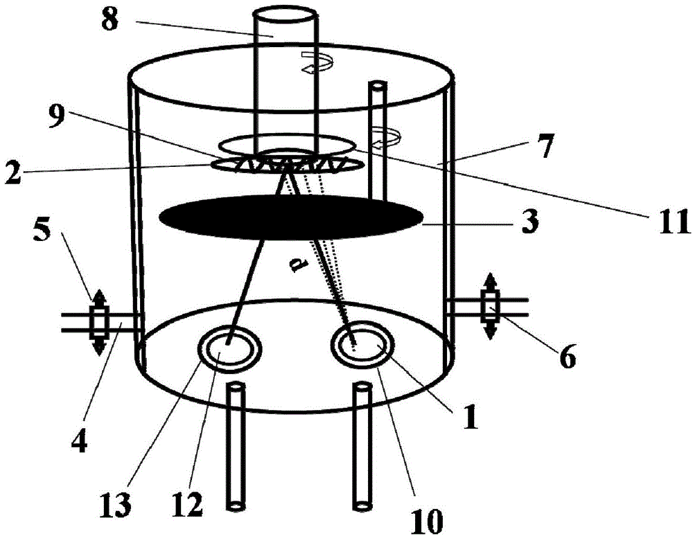
[0067] In the preparation method of the present invention, the distance d between the sample stage 2 and the radio frequency stage (sputtering source) 1, the sputtering pressure, the temperature of the substrate, and the size of the radio frequency power supply must be adjusted, and then the sputtering can be controlled to obtain the deposition on the conductive surface. The cadmium telluride nanowire array on the glass substrate makes the structure of the cadmium telluride nanorod array prepared by magnetron sputtering deposition uniform, effectively ensuring the uniform distribution of nano phases. The same principle is applicable to the preparation of layered bismuth telluride structure.

[0068] According to the results of experiments carried out by the inventors, when preparing CdTe nanorods, the preferred distance between the sample stage 2 and the radio frequency stage 1 is about 88-90mm, the preferred sputtering working pressure is about 0.4-0.5Pa, and the preferred rad...

Embodiment 1

[0070] (1) Preparation of cadmium telluride / bismuth telluride integrated nanostructure materials

[0071] Adjust the distance d=90mm between sample stage 2 and RF stage 1

[0072] Vacuumize the vacuum chamber 7 to make the vacuum degree in the vacuum chamber 7 reach 3.4×10 -4 Pa;

[0073] Turn on the heating control power supply 9, and turn on the sample rotation table 8, so that the substrate temperature rises to 350°C;

[0074] Fill the vacuum chamber 7 with argon, and adjust the air pressure to 0.4Pa;

[0075] Adjust the RF current to 140mA and the voltage to 0.60kV

[0076] Deposition time 2h;

[0077] After the preparation is complete, turn off the radio frequency power supply, cool naturally to room temperature 25°C, and take out the target;

[0078] Bi 2 Te 3 The target is placed on the DC platform, and the Te target is placed on the RF platform at the same time, and the vacuum chamber 7 is evacuated to make the vacuum degree in the vacuum chamber 7 reach 3.4×10 ...

Embodiment 2

[0091] (1) Preparation of cadmium telluride / bismuth telluride integrated nanostructure materials

[0092] Adjust the distance d=90mm between sample stage 2 and RF stage 1

[0093] Vacuumize the vacuum chamber 7 to make the vacuum degree in the vacuum chamber 7 reach 3.4×10 -4 Pa;

[0094] Turn on the heating control power supply 9, and turn on the sample rotation table 8, so that the substrate temperature rises to 400°C;

[0095] Rush into the vacuum chamber 7 with argon, and adjust the air pressure to 0.4Pa;

[0096] Adjust the RF current to 130mA and the voltage to 0.60kV

[0097] Deposition time 1.5h;

[0098] After the preparation is complete, turn off the radio frequency power supply, cool naturally to room temperature 25°C, and take out the target;

[0099] Bi 2 Te 3 The target is placed on the DC platform, and the Te target is placed on the RF platform at the same time, and the vacuum chamber 7 is evacuated to make the vacuum degree in the vacuum chamber 7 reach ...


PUM

PropertyMeasurementUnit
thicknessaaaaaaaaaa

Abstract

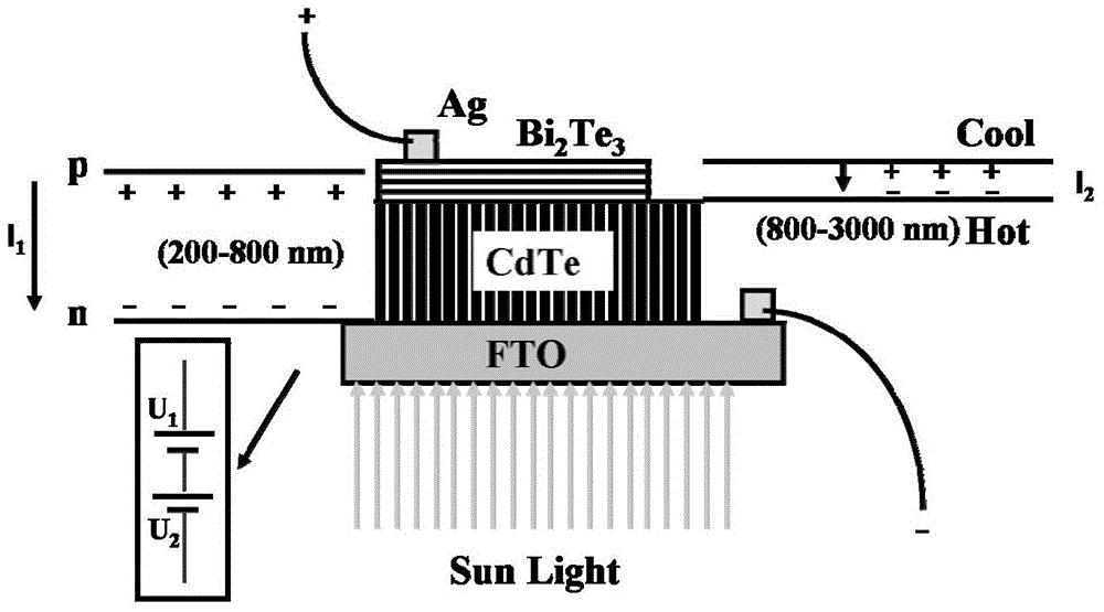
A cadmium telluride / bismuth telluride integrated nanostructure material with photothermal synergistic electricity. It deposits a layer of cadmium telluride nanorods on the conductive surface of a conductive glass substrate, and then deposits a layer of cadmium telluride nanorods on the surface of the cadmium telluride nanorod layer. A tellurium-doped bismuth telluride layer is deposited to form a cadmium telluride / bismuth telluride integrated nanostructure material. This material can simultaneously convert light and heat in the solar spectrum into electrical energy, achieving the effect of synergistic utilization and conversion of light and heat. The invention discloses its preparation method.

Description

technical field [0001] The invention relates to cadmium telluride (CdTe) / bismuth telluride (Bi 2 Te 3 ) Integrated materials and their preparation methods. Background technique [0002] As a clean and non-polluting new energy source, solar energy has received widespread attention as it bears the important task of national energy conservation and emission reduction under the background of vigorously advocating a low-carbon economy. 99% of the solar spectrum energy is concentrated in the ultraviolet to infrared band. Therefore, the photoelectric conversion technology of solar energy mainly includes photovoltaic cells using ultraviolet-visible spectrum and thermoelectric conversion using infrared heat energy. However, photovoltaic cells not only cannot absorb the infrared spectrum above 800nm ​​in the solar spectrum, but also the waste heat generated by the infrared spectrum will cause the overall temperature of the photovoltaic cell to rise, which in turn will cause the eff...

Claims


Application Information

Patent Timeline
Patent Type & Authority Patents(China)
IPC IPC(8): C23C14/06C23C14/35H01L31/18H01L35/34H10N10/01
CPCY02P70/50
Inventor 邓元罗柄威史永明祝薇叶慧红崔长伟
Owner 杭州知创新材料技术有限公司
Learn More