TSV process method without metal CMP

A process method and metal technology, which is applied in the field of metal-free CMP TSV process, can solve the problems of high barrier layer cost, expensive CMP equipment, high cost, etc., and achieve the effect of reducing cost, lowering the threshold of industrialization and manufacturing cost

Active Publication Date: 2015-07-08
NAT CENT FOR ADVANCED PACKAGING
View PDF1 Cites 0 Cited by
  • Summary
  • Abstract
  • Description
  • Claims
  • Application Information

AI Technical Summary

Problems solved by technology

Due to the high cost of CMP equipment and the high cost of barrier layer removal and redeposition process, the cost of this process remains high
The patent publication number is: EP1382065 A1 "Electropolishing metal layers on wafers having trenches or vias with dummy structure" discloses an electrochemical polishing technology for damascene process. The formation method does not mention the TSV process method of metal-free CMP

Method used


Image

  • TSV process method without metal CMP
  • TSV process method without metal CMP
  • TSV process method without metal CMP

Examples


Embodiment Construction

[0043] The present invention will be further described below in conjunction with specific drawings and embodiments.

[0044] A TSV process method free of metal CMP, comprising the following steps:

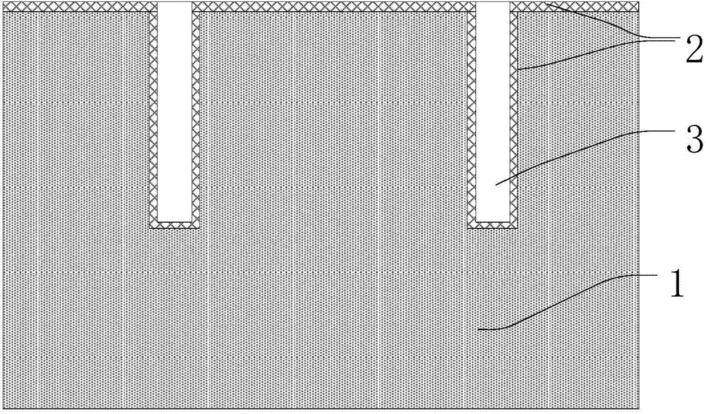
[0045] S1. If figure 1 As shown, a wafer 1 is provided as a substrate, a blind hole 3 (TSV hole) is formed in the wafer 1 by a deep reactive ion etching process, and an insulating layer 2 is formed on the upper surface of the wafer 1 and the inner wall of the blind hole 3 ;

[0046] The depth and diameter of the blind hole 3 can be determined according to specific requirements, and the aspect ratio is generally not less than 3:1. The material of the insulating layer 2 may be materials such as silicon dioxide, silicon nitride, silicon oxynitride, organic polymer, etc., and the layer structure may be a one-layer or multi-layer structure of the above materials.

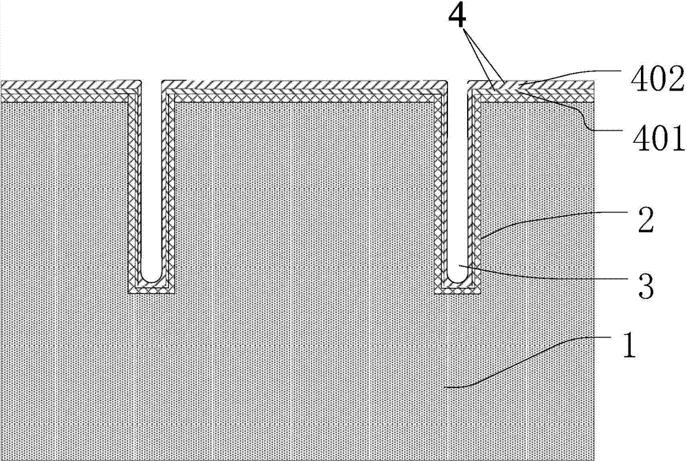
[0047] S2. If figure 2 As shown, a barrier layer 401 and a seed layer 402 are deposited on the upper surface of the wa...


PUM


Abstract

The invention provides a TSV process method without metal CMP. The method includes the steps that a wafer is provided to serve as a substrate, blind holes are formed in the wafer, and an insulating layer is manufactured on the upper surface of the wafer and the inner walls of the blind holes; a barrier layer and a seed layer are manufactured on the insulating layer of the upper surface of the wafer and the inner walls of the blind holes; second metal materials are filled in the blind holes; the second metal materials on the surface of the wafer in the filling process of the blind holes and the seed layer are removed by means of the electrochemical polishing technology; an annealing process is carried out on the wafer; a wet etching process is used for removing the barrier layer on the surface of the wafer; the electrochemical polishing technology is utilized to correct a step between the top of the second metal materials filled in the blind holes and the surface of the wafer; the surface of the wafer is uniformly coated by a first medium layer; imaging of the first medium layer is achieved, and a first medium later through hole is formed in the top of each blind hole; a first rewiring structure is formed on the first medium layer and the first medium layer through holes. According to the method, TSV process cost can be substantially reduced.

Description

technical field [0001] The invention relates to a packaging technology, in particular to a metal CMP-free TSV process method. Background technique [0002] At present, the mainstream process of TSV filling is to use copper electroplating process. The seed layer required by the electroplating process and the copper layer (surface copper) and barrier layer generated on the wafer surface during the electroplating process are removed by chemical mechanical polishing (CMP). , and then redeposit the barrier layer to make the rewiring structure. Because the CMP equipment is expensive, the cost of the removal and redeposition process of the barrier layer is high, so the cost of this process method remains high. The patent publication number is: EP1382065 A1 "Electropolishing metal layers on wafers having trenches or vias with dummy structure" discloses an electrochemical polishing technology for damascene process. The formation method does not mention the metal-free CMP TSV proces...

Claims


Application Information

Patent Timeline
Patent Type & Authority Patents(China)
IPC IPC(8): H01L21/768
Inventor 薛恺于大全
Owner NAT CENT FOR ADVANCED PACKAGING
Why Eureka
Try Eureka