Array substrate, manufacturing method thereof and display device

A technology for array substrates and manufacturing methods, applied in the display field, capable of solving problems such as array substrate crosstalk, greenish, and high common electrode resistance

Active Publication Date: 2013-12-25
BOE TECH GRP CO LTD
View PDF5 Cites 15 Cited by
  • Summary
  • Abstract
  • Description
  • Claims
  • Application Information

AI Technical Summary

Problems solved by technology

[0006] In order to solve the problems of crosstalk and greenish of the array substrate caused by the high resistance of the common electrode in the prior art, the present invention provides an array substrate, a manufacturing method thereof, and a display device, in order to reduce the phenomenon of crosstalk and greenish of the array substrate, and improve The picture quality of the display device provides a feasible technical solution

Method used


Image

  • Array substrate, manufacturing method thereof and display device
  • Array substrate, manufacturing method thereof and display device
  • Array substrate, manufacturing method thereof and display device

Examples


Embodiment Construction

[0055] In order to better understand the present invention, the present invention will be further described below in conjunction with the accompanying drawings and specific embodiments.

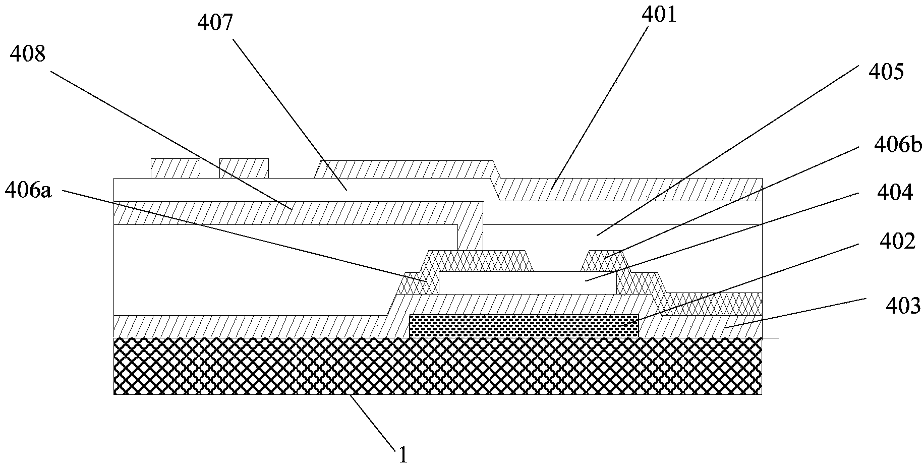
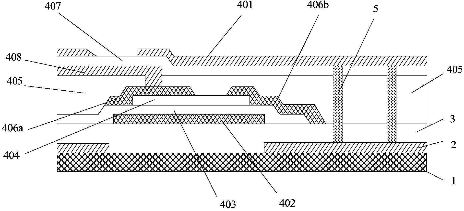
[0056] An embodiment of the present invention provides an array substrate, which includes a substrate and a common electrode layer on the substrate, and is characterized in that it also includes a conductive layer on a different layer from the common electrode layer, and the conductive layer is different from the common electrode layer. The common electrode layers are connected in parallel.

[0057] Wherein, the conductive layer may be located on the surface of the substrate, or the conductive layer is located on the surface of the gate insulating layer, and the common electrode layer is located in a different layer from the conductive layer.

[0058] It should be noted that, in the embodiment of the present invention, the position of the conductive layer is not limited to the surface of the ...


PUM


Abstract

The invention provides an array substrate, a manufacturing method thereof and a display device. The array substrate comprises a liner and a public electrode layer located on the liner. The array substrate is characterized by further comprising a conductive layer located on the surface of the liner, and the conductive layer and the public electrode layer are connected in parallel. The array substrate solves the problems that an existing public electrode is large in resistance and causes a crosstalk of an array substrate and a greenish phenomenon. Different from a mode that a public electrode with a single-layer transparent conductive film is used in the array substrate in the prior art, according to the technical scheme, the array substrate is additionally provided with a conductive layer, so that an equivalent resistor of the public electrode and an equivalent resistor of the conductive layer are in parallel, the resistance value of the public electrode is reduced, the crosstalk and greenish phenomena of the array substrate are reduced, and image quality of the display device is improved.

Description

technical field [0001] The present invention relates to the display field, in particular to an array substrate, a manufacturing method thereof, and a display device. Background technique [0002] Advanced Super Dimension Switch (ADS), its core technical characteristics are described as: through the electric field generated by the edge of the slit electrode in the same plane and the electric field generated between the slit electrode layer and the plate electrode layer to form a multi-dimensional The electric field makes all oriented liquid crystal molecules between the slit electrodes in the liquid crystal cell and directly above the electrodes rotate, thereby improving the working efficiency of the liquid crystal and increasing the light transmission efficiency. Advanced ultra-dimensional field conversion technology can improve the picture quality of thin film transistor liquid crystal display (Thin Film Transistor Liquid Crystal Display, TFT-LCD) products, with high resolu...

Claims


Application Information

Patent Timeline
Patent Type & Authority Applications(China)
IPC IPC(8): H01L27/12H01L21/77
CPCH01L27/124H01L27/1259
Inventor 张元波秦纬韩承佑马若玉
Owner BOE TECH GRP CO LTD
Why Eureka
Try Eureka