

PGA/BGA (Pin Grid Array/Ball Grid Array) three-dimensional structure for assembling components and production method thereof
A technology of three-dimensional structure and components, applied in the fields of semiconductor/solid-state device manufacturing, electrical components, electrical solid-state devices, etc., it can solve difficult coplanar welding of T/R modules, inability to assemble curved motherboards, and difficult welding of subsystems, etc. problems, resulting in improved reliability and performance, optimized lead lengths, and reduced system weight
- Summary
- Abstract
- Description
- Claims
- Application Information
AI Technical Summary
Problems solved by technology
Method used
Image

Examples
Embodiment 1
[0026] Example 1 ( The manufacturing method of the PGA / BGA three-dimensional structure of the present invention)
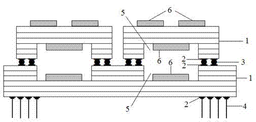
[0027] 1) By digging holes in the green tape, laminating the multi-layer green tape and then sintering to form the T / R module substrate with cavity and the subsystem substrate with cavity;
[0028] 2) Use AuSn solder sheet or solder paste to solder the PGA leads on the subsystem substrate, and the soldering temperature is 310-350°C;
[0029] 3) Use medium temperature solder with a melting point of 210-230°C to solder the components on the subsystem substrate through reflow soldering, and the soldering temperature is 240-270°C;
[0030] 4) On the T / R module substrate, place a medium-temperature solder ball with a melting point of 210-230°C on the BGA pad, use a medium-temperature solder paste with a melting point of 210-230°C to pre-fix the components in the cavity, and then pass Reflow soldering forms the BGA structure and soldering components on the T / R module...
PUM
 Abstract
Description
Claims
Application Information