A 1t1r array applied in fpga based on rram and its manufacturing method
A technology of 1T1R and manufacturing method, which is applied in the field of 1T1R array and its manufacturing, and can solve problems such as single logic function and inability to complete complex logic functions.
- Summary
- Abstract
- Description
- Claims
- Application Information
AI Technical Summary
Problems solved by technology
Method used
Image

Examples
Embodiment 1
[0053] In order to solve the problem that the existing 1T1R array can realize a single logic function and cannot complete complex logic functions, this embodiment provides a 1T1R array based on RRAM applied in FPGA, which is applied to devices such as storage devices. The 1T1R array includes:
[0054] Logic circuit, used to realize the set logic function;
[0055] A signal input circuit is connected to the logic circuit and provides signals for the logic circuit;
[0056] a signal output circuit for outputting the signal of the logic circuit;
[0057] The logic circuits are connected in parallel.
[0058] The invention can set the logic circuit as required, and realize complex logic functions through the connection relationship between the logic circuit and the signal output circuit.
[0059] In practice, power supply and current limiting resistors are also included for specific applications. The power supply is used to provide electric energy for the logic circuit; the cu...
Embodiment 2
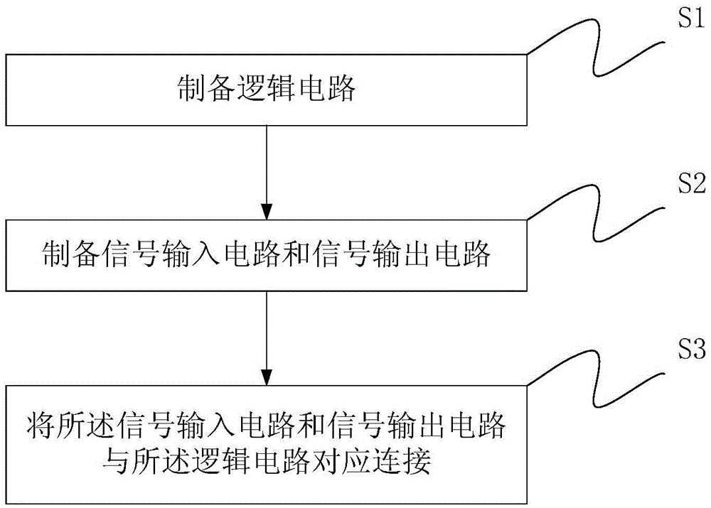
[0064] This embodiment and Embodiment 1 belong to the same inventive concept. This embodiment provides a method for manufacturing a 1T1R array based on RRAM applied in FPGA, the method includes the following steps, such as figure 2 Shown:
[0065] S1: preparing a logic circuit;
[0066] S2: preparing a signal input circuit and a signal output circuit;
[0067] In practice, logic circuits, signal input circuits and signal output circuits can be fabricated on one substrate.
[0068] S3: Correspondingly connecting the signal input circuit and the signal output circuit to the logic circuit. The corresponding connection refers to connecting the signal input circuit, the signal output circuit and the logic circuit as required, so that the signal output circuit outputs the required signal.
[0069] In practice, the logic circuit is usually prepared first, and then the signal input circuit and signal output circuit are prepared. by image 3 As an example, the logic circuit prepar...
Embodiment 3
[0081] The present invention will be described in detail below through an actual scene.
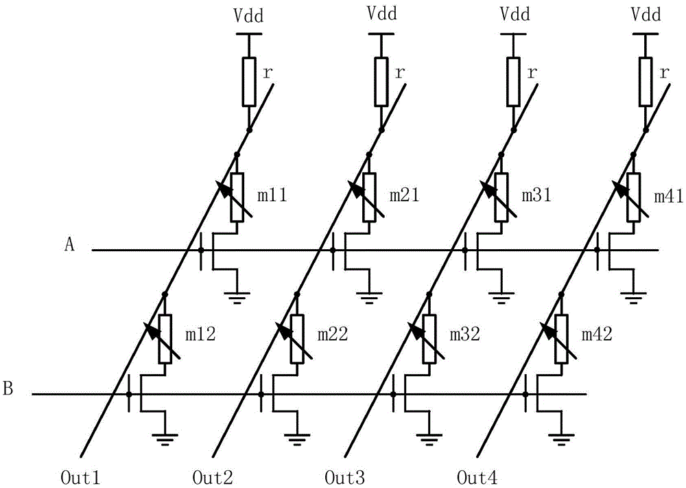
[0082] figure 1 It is the structure diagram of 1T1R unit in the present invention including two 1T1R, wherein, Vdd is the power supply; r is the current limiting resistor; OUT1, OUT2, OUT3, OUT4 are the output terminals of the signal output circuit; m11, m21, m31, m41, m12 , m22, m32, m42 are resistive variable resistors.
[0083] figure 1 In, the output terminal can form the following logic according to the input A, B signal and RRAM on-off, such as OUT 1 = m 11 ‾ · m 12 ‾ + m 11 ‾ · m 12 · B ‾ + m 12 ‾ ...
PUM
 Abstract
Description
Claims
Application Information
 - R&D
- Intellectual Property
- Life Sciences
- Materials
- Tech Scout
- Unparalleled Data Quality
- Higher Quality Content
- 60% Fewer Hallucinations
Browse by: Latest US Patents, China's latest patents, Technical Efficacy Thesaurus, Application Domain, Technology Topic, Popular Technical Reports.
© 2025 PatSnap. All rights reserved.Legal|Privacy policy|Modern Slavery Act Transparency Statement|Sitemap|About US| Contact US: help@patsnap.com