Pixel unit of CMOS image sensor

An image sensor and pixel unit technology, applied in image communication, electrical components, color TV components, etc., can solve the problem of not being able to achieve high sensitivity and high dynamics at the same time

Active Publication Date: 2014-01-01
SHANGHAI INTEGRATED CIRCUIT RES & DEV CENT
View PDF7 Cites 8 Cited by
  • Summary
  • Abstract
  • Description
  • Claims
  • Application Information

AI Technical Summary

Problems solved by technology

However, the pixel unit in the prior art can only meet one of the indicators of high sensitivity and high dynamic range, but cannot simultaneously achieve the two indicators of high sensitivity and high dynamic range

Method used


Image

  • Pixel unit of CMOS image sensor
  • Pixel unit of CMOS image sensor
  • Pixel unit of CMOS image sensor

Examples


Embodiment Construction

[0032] The implementation of the present invention will be described in detail below in conjunction with the drawings and examples, so that the realization process of how to use technical means to solve technical problems and achieve technical effects in the present invention can be fully understood and implemented accordingly.

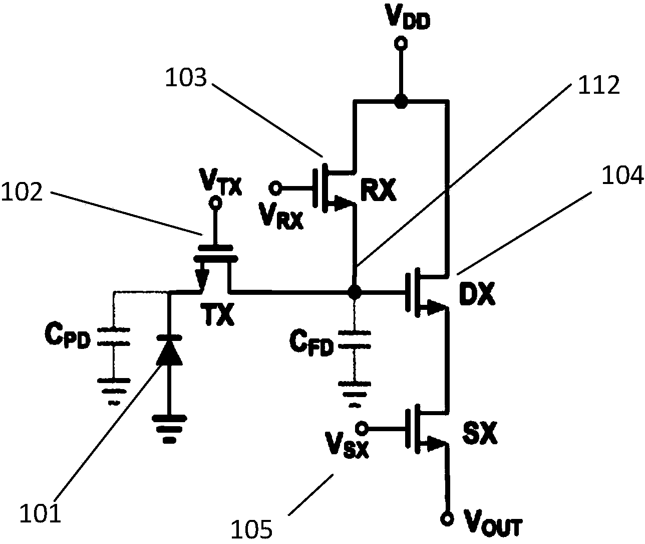
[0033] In the following embodiments of the present invention, according to the illuminance of incident light, the transmission tubes with corresponding transmission efficiency of the transmission tube group are selectively activated to transmit the electrons, so that the electrons are transmitted from the source terminal of the transmission tube group to the drain terminal and converts to a voltage signal.

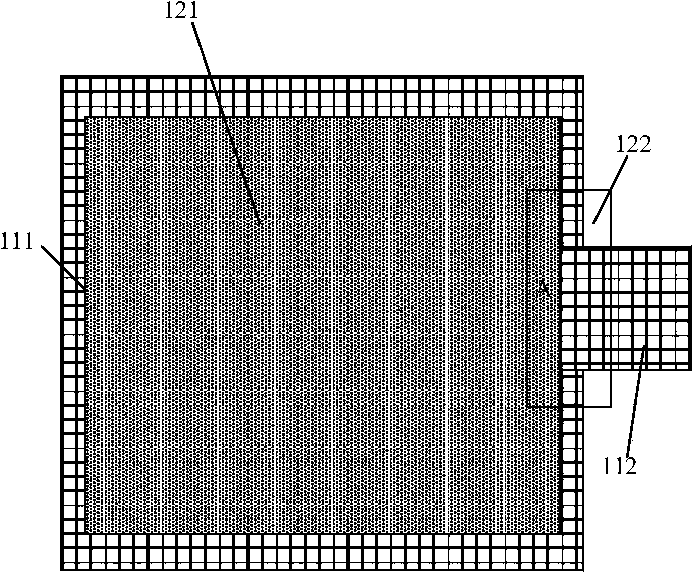
[0034] Figure 4 is the circuit structure of the pixel unit of the CMOS image sensor in Embodiment 1 of the present invention, Figure 5 It is the layout structure of the pixel unit of the CMOS image sensor in the first embodiment of the present ...


PUM


Abstract

The invention discloses a pixel unit of a CMOS image sensor and a manufacturing method of the pixel unit and belongs to the technical field of semiconductors. The pixel unit comprises a photosensitive diode and a pass transistor set. The pass transistor set comprises a plurality of pass transistors which are connected at the source electrode end and the drain electrode end in parallel respectively. The grid electrode of each pass transistor and an injection area of the photosensitive diode form an overlapping are, wherein the overlapping areas are different in size, so that different transmission efficiencies are achieved. The photosensitive diode is used for conducting photovoltaic conversion so that a photon can be converted into an electron. The pass transistor set is used for achieving the purpose that the pass transistor corresponding to the transmission efficiency is selectively started according to the illuminance of incident light, so that electron transmission is conducted, and therefore the electron is transmitted to the drain electrode end from the source electrode of the pass transistor set and converted into a voltage signal. According to the pixel unit of the CMOS image sensor, the pass transistor, corresponding to the transmission efficiency, of the pass transistor set is selectively started according to the illuminance of incident light, so that electron transmission is conducted, and therefore the index of high sensitivity and the index of high dynamic are achieved.

Description

technical field [0001] The invention belongs to the field of integrated circuits, and in particular relates to a pixel unit of a CMOS image sensor. Background technique [0002] An image sensor refers to a device that converts optical signals into electrical signals. Image sensors include charge-coupled devices (Charge-coupled Device, hereinafter referred to as CCD image sensors) and complementary metal oxide semiconductor image sensors (CMOS IMAGE SENSOR, hereinafter referred to as CIS image sensors). [0003] Compared with CCD image sensors, CMOS image sensors have the characteristics of low power consumption, low cost, and compatibility with CMOS technology, so they are more and more widely used. CMOS image sensors are not only used in consumer electronics, such as miniature digital cameras (DSC), mobile phone cameras, video cameras, and digital single-lens reflex cameras (DSLR), but also in automotive electronics, video surveillance, biotechnology, and medicine. [000...

Claims


Application Information

Patent Timeline
Patent Type & Authority Applications(China)
IPC IPC(8): H04N5/374H01L27/146
Inventor 顾学强周伟肖慧敏
Owner SHANGHAI INTEGRATED CIRCUIT RES & DEV CENT
Why Eureka
Try Eureka