Surface plasmon imaging photoetching structure

A surface plasmon and imaging technology, which is used in microlithography exposure equipment, photolithography process exposure devices, etc. It is difficult to break through the resolution and other issues to achieve the effect of high lithography resolution

Inactive Publication Date: 2014-01-08
ANHUI NORMAL UNIV
View PDF8 Cites 8 Cited by
  • Summary
  • Abstract
  • Description
  • Claims
  • Application Information

AI Technical Summary

Problems solved by technology

However, due to the limitation of the diffraction limit, the improvement of lithography resolution is limited by the exposure wavelength, it is difficult to break through the half-wavelength resolution, and it is impossible to achieve nanometer-scale lithography

Method used


Image

  • Surface plasmon imaging photoetching structure

Examples


Embodiment Construction

[0013] The present invention will be further described below in conjunction with drawings and embodiments.

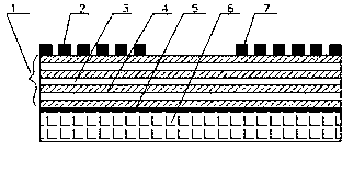
[0014] like figure 1 As shown, the present invention consists of a superlens structure (1), a first grating (2), a resist layer (5), a substrate (6) and a second grating (7). The first grating (2) and the second grating (7) are located above the super lens structure (1), and the resist layer (5) is located below the super lens structure (1). The super lens structure (1) is composed of multilayer dielectric films (3) and multilayer metal films (4) alternately. When the first grating (2), the second grating (7) are made of gold, the material of the dielectric film (3) is silicon dioxide, and the material of the metal film (4) is gold or silver or aluminum, the dielectric film (3) and the metal film (4) When the thickness is 10nm~100nm, it is a surface plasmon imaging lithography structure for i-line 365nm lithography.

[0015] When illuminated by a 365nm ultraviolet li...


PUM

PropertyMeasurementUnit
thicknessaaaaaaaaaa
thicknessaaaaaaaaaa
thicknessaaaaaaaaaa

Abstract

The invention discloses a surface plasmon imaging photoetching structure which is characterized by comprising a super lens structure (1), a first optical grating (2), a corrosion-resistant agent layer (5), a substrate (6) and a second optical grating (7). The first optical grating (2) and the second optical grating (7) are positioned on the upper side of the super lens structure (1), and the corrosion-resistant agent layer (5) is positioned on the lower side of the super lens structure (1). The surface plasmon imaging photoetching structure has the advantages that SPPs (surface plasmon polaritons) can be excited by the optical gratings from two ends of the surface plasmon imaging photoetching structure and are interfered with one another to form interference fringes, evanescent waves are amplified by the super lens structure, super-resolution images can be formed on corrosion-resistant agents, and accordingly exposure is further completed; short wavelength characteristics of the SPPs are sufficiently utilized, and the super-resolution ability of super lenses is utilized, so that the photoetching resolution is super high; far-field imaging photoetching can be implemented, and the focal depth can be improved advantageously.

Description

technical field [0001] The invention relates to a surface plasmon imaging photolithography structure, which belongs to the technical field of semiconductor optoelectronic devices. Background technique [0002] Photolithography technology is a typical technology for microfabrication of semiconductor devices. With the continuous development of science and technology, the size of devices is getting smaller and higher, and the degree of integration is getting higher and higher. The resolution requirements of photolithography technology are also getting higher and higher. However, due to the limitation of the diffraction limit, the improvement of lithography resolution is limited by the exposure wavelength, and it is difficult to break through the half-wavelength resolution, and it is impossible to achieve nanometer lithography. In recent years, the research on metal surface plasmonic SPPs has made great progress. SPP refers to the collective oscillation of free electrons on the...

Claims


Application Information

Patent Timeline
Patent Type & Authority Applications(China)
IPC IPC(8): G03F7/20
Inventor 石建平米佳佳张青张颖姚敏
Owner ANHUI NORMAL UNIV
Why Eureka
Try Eureka