Cell-based hierarchical optical proximity correction (OPC) method

A technology of optical proximity effect and correction method, which is applied in optics, original parts for photomechanical processing, microlithography exposure equipment, etc., can solve problems such as low chip production efficiency and cumbersome full-chip OPC correction methods, and achieve improved chip performance. Production efficiency, reduction of storage capacity, and reduction of production errors

Active Publication Date: 2012-10-03
佛山中科芯蔚科技有限公司
View PDF0 Cites 0 Cited by
  • Summary
  • Abstract
  • Description
  • Claims
  • Application Information

AI Technical Summary

Problems solved by technology

[0010] In order to solve the problem of cumbersome full-chip OPC correction method and low chip production efficiency in the prior art, the present invention provides a hierarchical optical proximity effect correction method based on Cell

Method used


Image

  • Cell-based hierarchical optical proximity correction (OPC) method
  • Cell-based hierarchical optical proximity correction (OPC) method
  • Cell-based hierarchical optical proximity correction (OPC) method

Examples


Embodiment Construction

[0025] In order to make the object, technical solution and advantages of the present invention clearer, the present invention will be described in further detail below in conjunction with specific embodiments and with reference to the accompanying drawings.

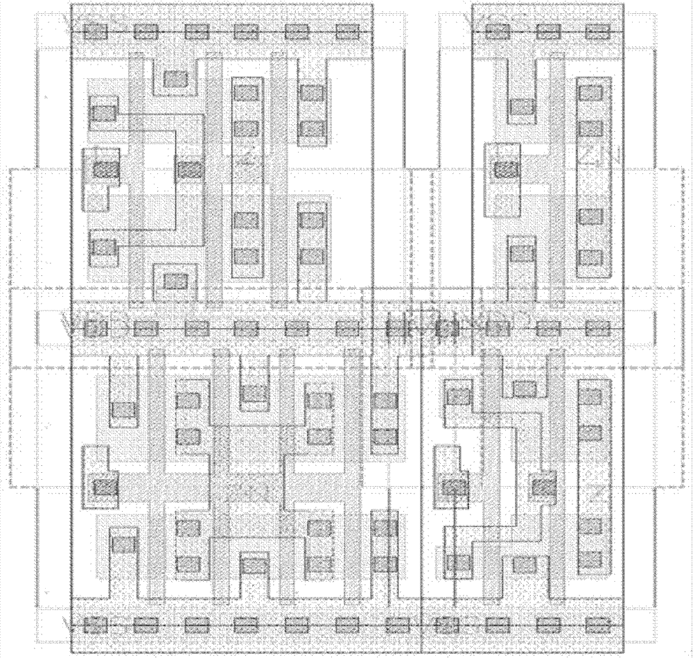
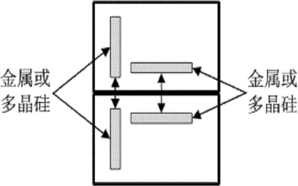
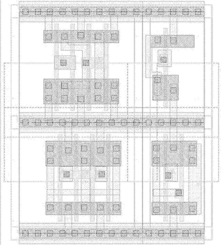
[0026] The hierarchical optical proximity effect correction method based on Cell provided by the present invention is to regularize the graphics of all standard cells, so that the height of the standard cells is equal, and the width is Wt, 2Wt. In this way, the layout is neatly spliced ​​without gaps, reducing The uncertainty of the lithography environment caused by the splicing gap of the traditional standard cell is eliminated, and the adjacent environment of the standard cell library is predictable, which is beneficial to OPC. Perform OPC processing on the standard unit during the construction of the standard unit.

[0027] see figure 1 , although the height of the traditional standard cells is consistent, but their w...


PUM


Abstract

The invention relates to the technical field of a manufacturing process and layout design of a 65-nanometre integrated circuit and discloses a cell-based hierarchical optical proximity correction (OPC) method. The method comprises the following steps of: regularizing graphs of all standard units by introducing a concept of hierarchical design into full-chip OPC process; carrying out OPC on the standard units in the process of construction of a standard unit library; and replacing part of the standard units by units which are subjected to the OPC after a full-chip layout is obtained, so that the OPC in a full-chip planishing mode is not required, the data storage content of a mask is reduced greatly, a photoetching resolution can be improved conveniently, a production error is further reduced, and the production efficiency of a chip is improved.

Description

technical field [0001] The invention relates to the technical field of 65nm integrated circuit manufacturing technology and layout design, in particular to a Cell-based hierarchical optical proximity correction (Optical Proximity Correction, OPC) method. Background technique [0002] The integrated circuit (Integrated Circuit, IC) manufacturing technology develops rapidly at a speed of doubling the integration level every 18 months according to or even exceeding Moore's Law. However, when the feature size of integrated circuits drops below 100 nanometers, IC manufacturing technology encounters unprecedented challenges, and one of the important aspects comes from the lithography process in manufacturing. The feature size of the chip has been reduced to be smaller than the wavelength of the lithography light source. Due to the diffraction effect, the error of the lithography instrument and the low-pass filtering effect of the lens, the pattern on the wafer cannot be consistent...

Claims


Application Information

Patent Timeline
Patent Type & Authority Patents(China)
IPC IPC(8): G03F1/36G03F7/20
Inventor 罗海燕陈岚尹明会赵劼
Owner 佛山中科芯蔚科技有限公司
Why Eureka
Try Eureka