Array substrate, array substrate driving method and display device

一种阵列基板、显示装置的技术,应用在静态指示器、仪器、电数字数据处理等方向,能够解决降低产品良率、增加工艺步骤、制程重复等问题,达到降低生产成本、节约电极材料、提高产品良率的效果

Active Publication Date: 2014-01-08
BOE TECH GRP CO LTD
View PDF4 Cites 37 Cited by
  • Summary
  • Abstract
  • Description
  • Claims
  • Application Information

AI Technical Summary

Problems solved by technology

[0004] The structure of the display device in which the display screen and the touch screen are made separately has a variety of separate electrodes (pixel electrodes in the display screen, sensing electrodes and driving electrodes in the touch screen), resulting in the There are many manufacturing process steps and the process is repeated, resulting in waste of electrode materials and processes, resulting in an increase in the production cost of the display device; at the same time, the display screen and touch screen require subsequent assembly, which further increases the process steps and reduces the product yield.

Method used


Image

  • Array substrate, array substrate driving method and display device
  • Array substrate, array substrate driving method and display device
  • Array substrate, array substrate driving method and display device

Examples


Embodiment 1

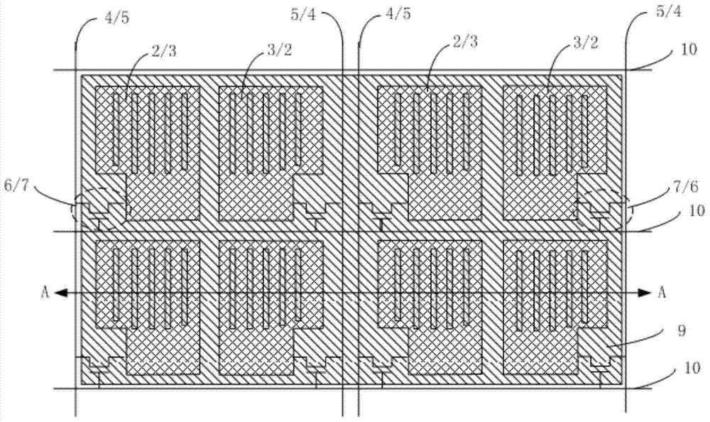
[0036] Such as figure 1 , 2 As shown, this embodiment provides an array substrate, the array substrate includes a display area and a non-display area, multiple sets of source lines and multiple gate lines are arranged in the display area, multiple sets of source lines and multiple gate lines The lines intersect and divide the display area into a plurality of pixel areas, the first electrode 2 and the second electrode 3 are arranged in the pixel area, the first electrode 2 and the second electrode 3 are adjacent and electrically isolated, the first electrode 2 and the second electrode The two electrodes are time-divisionally multiplexed into pixel electrodes for display, sensing electrodes and driving electrodes for touch control.

[0037] combine figure 1 with figure 2 , a group of source lines includes a first source line 4 and a second source line 5, a first thin film transistor 6 and a second thin film transistor 7 are arranged in the pixel area, the drain of the first ...

Embodiment 2

[0069] Such as Figure 5 As shown, the difference between this embodiment and Embodiment 1 is that in this embodiment, the display device still includes the first electrode 2, the second electrode 3 and the common electrode 9, and the first electrode 2 and the second electrode 3 are still arranged on The common electrode 9 is disposed on the array substrate 11 , and the common electrode 9 is disposed on the color filter substrate 12 . The common electrode 9 at least partially overlaps with the first electrode 2 and the second electrode 3 in the orthographic projection direction.

[0070] That is, the display device of this embodiment is a TN (Twisted Nematic, twisted nematic) mode, VA (Vertical Alignment, vertical alignment) mode liquid crystal display device.

[0071] The structure of the array substrate 11 in this embodiment is the same as the structure of the array substrate 11 in Embodiment 1 except that the common electrode 9 and the insulating layer 8 corresponding to th...

Embodiment 3

[0073] The difference between this embodiment and Embodiments 1 and 2 is that, in this embodiment, the display device includes a first electrode and a second electrode, and the first electrode and the second electrode are arranged on the array substrate and serve as OLED (Organic Light -Emitting Diode: the anode electrode of an organic light-emitting diode).

[0074] That is, the display device of this embodiment is an AMOLED (Active Matrix OLED, active matrix driven organic light emitting diode) display device. Since the OLED itself can emit light, compared with the liquid crystal display devices in Embodiments 1 and 2, no backlight source 13 is required in this display device.

[0075]The structure of the array substrate in this embodiment is the same as the structure of the array substrate in Embodiment 2 except that the first electrode and the second electrode are directly set as the anode electrodes of the two OLEDs in the same pixel area; at the same time, the display T...


PUM


Abstract

The invention relates to the field of displaying, in particular to an array substrate, an array substrate driving method and a display device comprising the array substrate. The array substrate comprises a display area and a non-display area; the display area is internally provided with multiple groups of source lines and a plurality of grid lines, and the groups of source lines and the grid lines are crossed and partition the display area into a plurality of pixel areas, wherein each pixel area is internally provided with a first electrode and a second electrode, and the first electrodes and the second electrodes are adjacent and electrically isolated. The array substrate provided by the invention carries out time division multiplexing on the two electrodes in the same pixel area to form a pixel electrode for displaying, a induction electrode for touch control and a driving electrode for touch control, so that the technical steps of the array substrate are reduced, the electrode materials are saved, and the product cost is reduced.

Description

technical field [0001] The present invention relates to the display field, in particular, to an array substrate, a driving method for the array substrate, and a display device including the array substrate. Background technique [0002] Touch screen is the latest information input device at present. It can realize human-computer interaction simply, conveniently and naturally, and provide people with a brand-new method of multimedia human-computer interaction. The earth satisfies people's visual and tactile enjoyment. [0003] At present, touch screens can be divided into three types according to their composition: Add on Mode Touch Panel, On Cell Touch Panel and In Cell Touch Panel. . According to the different structures of the touch screen, there are various design schemes for the touch screen. Taking the liquid crystal display device with touch function as an example, it is more common to manufacture the display screen and the touch screen of the liquid crystal display ...

Claims


Application Information

Patent Timeline
Patent Type & AuthorityApplications(China)
IPC IPC(8): H01L27/12G06F3/041G09G3/20G09G3/36
CPCG06F3/0412G06F3/04184G06F3/0443G09G3/20G09G2300/0804G09G2310/08H01L27/12
Inventor程鸿飞张玉欣
OwnerBOE TECH GRP CO LTD