Novel compound semiconductor and usage for same

一种半导体、化合物的技术,应用在新型化合物半导体材料领域

Active Publication Date: 2014-01-08
LG CHEM LTD
View PDF8 Cites 4 Cited by
  • Summary
  • Abstract
  • Description
  • Claims
  • Application Information

AI Technical Summary

Problems solved by technology

However, many conventional compound semiconductors cannot satisfy all these conditions simultaneously

Method used


Image

  • Novel compound semiconductor and usage for same

Examples


Embodiment

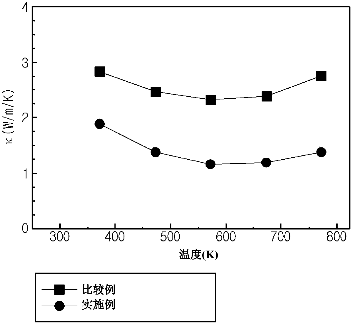
[0066] Prepare 0.1727g In, 1.3121g Co, 8.1329g Sb, 0.2375g Se and 0.1449g Co 3 o 4 As a reagent, and use a mortar and mortar for mixing. The material mixed as above was put into a quartz tube and vacuum-sealed, then heated at 650 °C for 36 hours. The time taken to raise the temperature to 650°C was 1 hour and 30 minutes, and In 0.25 co 4 Sb 11 o 0.5 Se 0.5 powder.

[0067] Part of the composite material produced above was formed into a disk having a diameter of 10 mm and a thickness of 1 mm. Thereafter, a pressure of 200 MPa was applied to the disk using CIP (cold isostatic pressing). Next, the resulting product was put into a quartz tube and vacuum sintered for 12 hours.

[0068] For the sintered discs, thermal conductivity (κ) was measured at pre-set temperature intervals using LFA457 (Netzsch, Inc). The measurement results are shown as examples in figure 1 middle.


PUM


Abstract

Disclosed are new compound semiconductors which may be used for solar cells or as thermoelectric materials, and their application. The compound semiconductor may be represented by a chemical formula: InxCo4Sb12-n-zQ'nSez, where Q' is at least one selected from the group consisting of O and S, 0<x@0.5, 0<n@2 and 0@z<2.

Description

technical field [0001] The present disclosure relates to a novel compound semiconductor material that can be used in solar cells or as a thermoelectric material, as well as the preparation method and use of the material. [0002] This application claims Korean Patent Application No. 10-2011-0045348 filed on May 13, 2011 in Korea, Korean Patent Application No. 10-2011-0045349 filed on May 13, 2011 and Korean Patent Application No. 10-2011-0045349 filed on May 13, 2011 and Korean Patent Application No. 10-2011-0049609 filed on May 11, 2012 and Korean Patent Application No. 10-2012-0050259 filed on May 11, 2012, the entire contents of these four patent applications are incorporated herein by reference middle. Background technique [0003] A compound semiconductor is not a single element such as silicon and germanium, but a compound containing two or more composite elements serving as semiconductors. Various compound semiconductors have been developed and used in many fields. ...

Claims


Application Information

Patent Timeline
Patent Type & Authority Applications(China)
IPC IPC(8): C01B19/00C01G15/00C01G51/00C01G30/00H01L31/032
CPCC01B19/002C01G51/006H01L35/18C01P2006/40H01L31/032C01P2002/54H10N10/853C01B19/00C01G15/00C01G51/00C01G30/00
Inventor 朴哲凞金兑训
Owner LG CHEM LTD
Why Eureka
Try Eureka