Preparation method of high-purity copper target material

A high-purity copper and target material technology, applied in the field of semiconductor sputtering, can solve problems such as unsatisfactory

Active Publication Date: 2014-01-15
KONFOONG MATERIALS INTERNATIONAL CO LTD
View PDF4 Cites 23 Cited by
  • Summary
  • Abstract
  • Description
  • Claims
  • Application Information

AI Technical Summary

Problems solved by technology

For this demand in the semiconductor industry, the tradition

Method used


Image

  • Preparation method of high-purity copper target material
  • Preparation method of high-purity copper target material
  • Preparation method of high-purity copper target material

Examples


Embodiment Construction

[0028] In order to make the above-mentioned objects, features and advantages of the present invention more obvious and understandable, the specific embodiments of the present invention will be described in detail below with reference to the accompanying drawings. Since the present invention focuses on explaining the principle, the drawings are not drawn to scale.

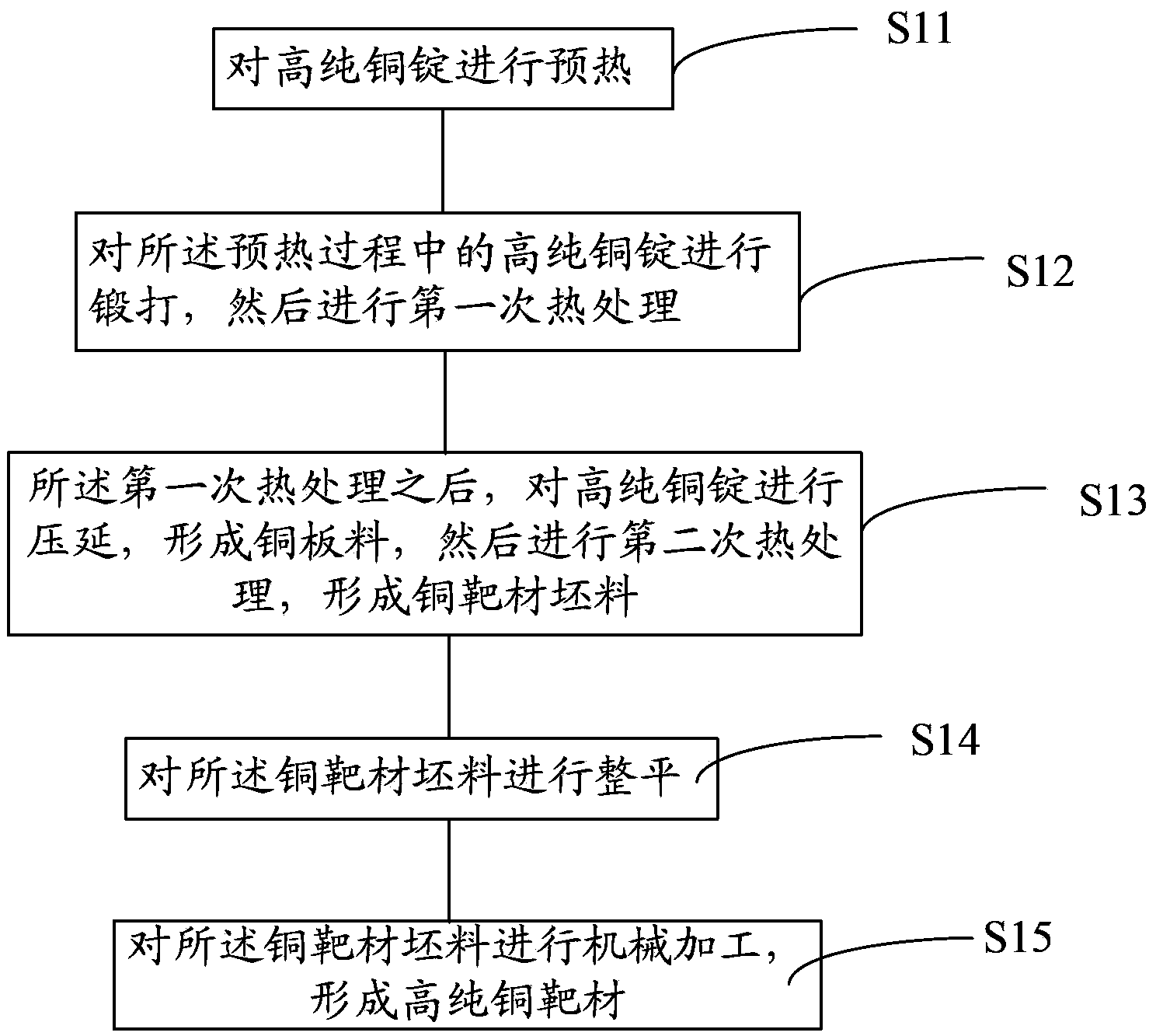
[0029] figure 1 Shown is the flow chart of the preparation method of the high-purity copper target provided by this embodiment, figure 2 for figure 1 The structure diagram corresponding to the middle forging process. The following is a specific introduction.

[0030] Step S11 is executed to preheat the high-purity copper ingot.

[0031] The general purity of the semiconductor copper target is required to be above 3N (99.99%), such as 4N5 (99.995%) or 5N (99.999%). Therefore, the purity of the high-purity copper ingot used is above 4N (99.99%), and in this embodiment, it is preferably a 4N5 (99.995%) copper ingot. In th...


PUM

PropertyMeasurementUnit
Grain sizeaaaaaaaaaa

Abstract

The invention relates to a preparation method of a high-purity copper target material. The preparation method comprises the steps of preheating a high-purity copper ingot; forging the high-purity copper ingot in the preheating process and performing heat treatment for the first time; calendering the high-purity copper ingot subjected to heat treatment for the first time to form a copper plate material, and performing heat treatment for the second time to form a copper target blank; machining the copper target blank to form the high-purity copper target material. The high-purity copper target material with the grain size being less than 100 microns and an excellent spattering direction can be manufactured by adopting the technical scheme of the invention.

Description

Technical field [0001] The invention relates to the field of semiconductor sputtering, in particular to a method for preparing a high-purity copper target material. Background technique [0002] The sputtering target is an extremely important key material necessary for the manufacture of semiconductor chips. The principle of using it to make devices is to use physical vapor deposition technology (PVD) to bombard the target with high-pressure accelerated gaseous ions, so that the atoms of the target are It is sputtered out and deposited on a silicon wafer in the form of a thin film to finally form a complex wiring structure in the semiconductor chip. Sputtering targets have many advantages such as the uniformity and controllability of metal coatings, and are widely used in the semiconductor field. With the rapid development of the semiconductor industry, compared with the traditional interconnect material aluminum, copper has higher conductivity and better resistance to electromi...

Claims


Application Information

Patent Timeline
IPC IPC(8): C23C14/34C22F1/08
Inventor 姚力军相原俊夫大岩一彦潘杰王学泽高建
Owner KONFOONG MATERIALS INTERNATIONAL CO LTD
Why Eureka
Try Eureka